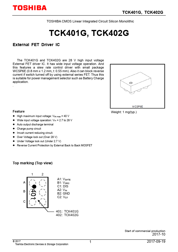
| Part | TCK401G |
|---|---|
| Description | External FET Driver IC |
| Manufacturer | Toshiba |
| Size | 499.27 KB |
Pricing from 0.1872 USD, available from Avnet and Verical.
Price & Availability
| Seller | Inventory | Price Breaks | Buy |
|---|---|---|---|
| Avnet | 15000 | 5000+ : 0.1872 USD 10000+ : 0.1856 USD 20000+ : 0.18296 USD 40000+ : 0.18032 USD |
View Offer |
| Verical | 2188 | 27+ : 0.0996 USD 100+ : 0.0976 USD 250+ : 0.0955 USD 500+ : 0.0934 USD |
View Offer |
Related Datasheets
| Part Number | Manufacturer | Description |
|---|---|---|
| LTH7R | FINE MADE ELECTRONICS | Charger management IC |
| MT6835 | MagnTek | 21-Bit High Accuracy Magnetic Angle Encoder IC |
| EG1000AE | Yige | linear constant current IC |
