TC74AC273P Description
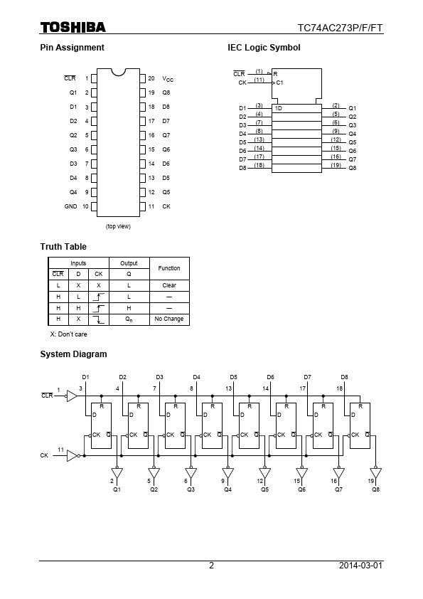
It achieves the high speed operation similar to equivalent Bipolar Schottky TTL while maintaining the CMOS low power dissipation. Information signals applied to D inputs are transferred to the Q output on the positive going edge of the clock pulse. When the CLR input is held “L”, the Q outputs are at a low logic level independent of the other inputs.
TC74AC273P Key Features
- High speed: fmax = 170 MHz (typ.) at VCC = 5 V
- Low power dissipation: ICC = 8 μA (max) at Ta = 25°C
- High noise immunity: VNIH = VNIL = 28% VCC (min)
- Symmetrical output impedance
- Balanced propagation delays: tpLH ∼- tpHL
- Wide operating voltage range: VCC (opr) = 2 V to 5.5 V
- Pin and function patible with 74F273