TC74HC112AF Description
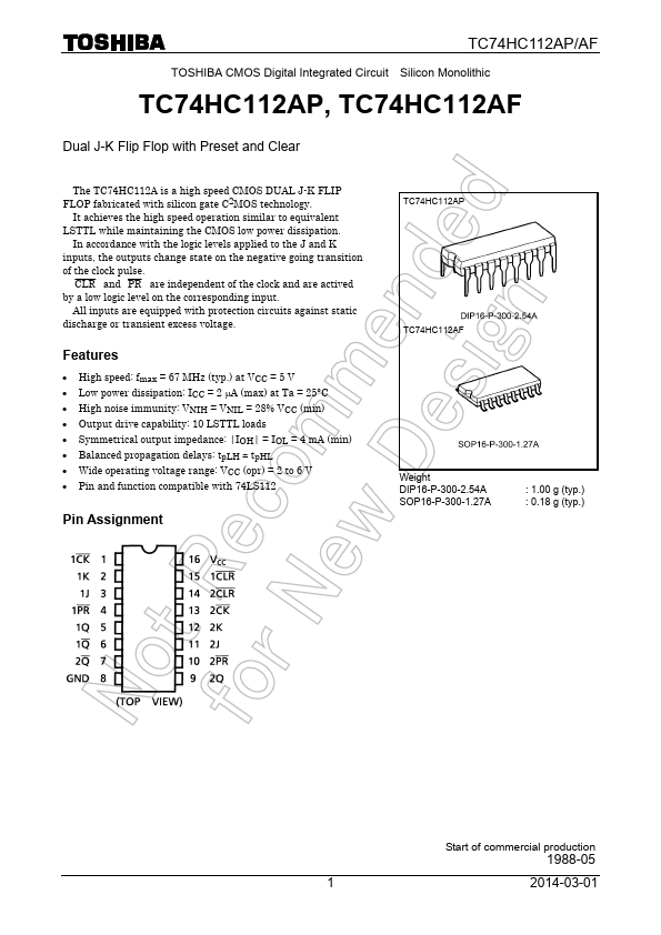
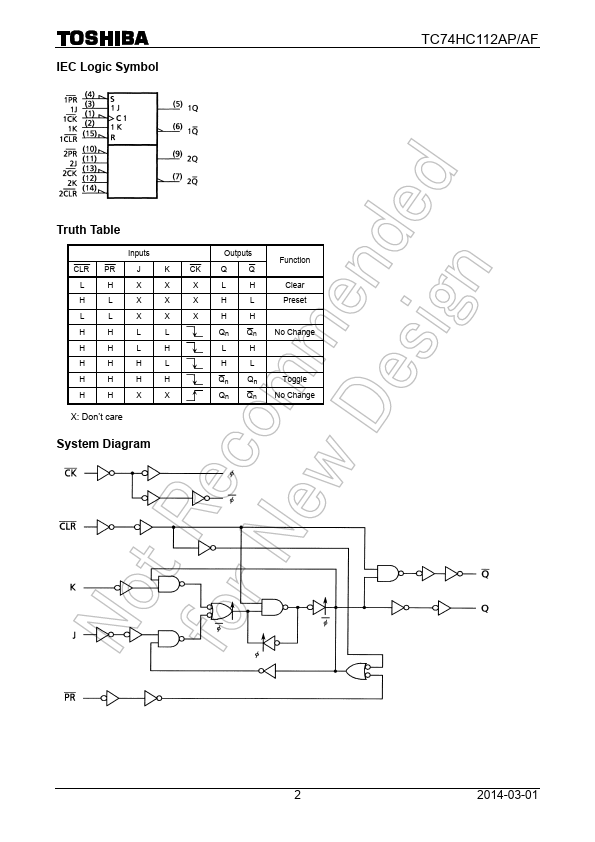
It achieves the high speed operation similar to equivalent LSTTL while maintaining the CMOS low power dissipation. In accordance with the logic levels applied to the J and K inputs, the outputs change state on the negative going transition of the clock pulse. CLR and PR are independent of the clock and are actived by a low logic level on the corresponding input.
TC74HC112AF Key Features
- High speed: fmax = 67 MHz (typ.) at VCC = 5 V Low power dissipation: ICC = 2 μA (max) at Ta = 25°C High noise immunity:
- Wide operating voltage range: VCC (opr) = 2 to 6 V Pin and function patible with 74LS112
- http://..net/
- http://..net/