TPD1032F Description
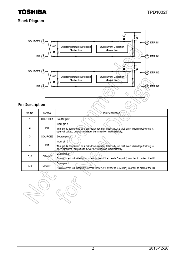
Source pin 2 Input pin 2 This pin is connected to a pull-down resistor internally, so that even when input wiring is open-circuited, output can never be turned on inadvertently. Drain pin 2 Drain current is limited (by current limiter) if it exceeds 3 A (min) in order to protect the IC. Drain pin 1 Drain current is limited (by current limiter) if it exceeds 3 A (min) in order to protect the IC.
TPD1032F Key Features
- Two built-in power IC chips with a new structure bining a control block and a vertical power MOSFET (L2-π-MOS) on each c
- Can directly drive a power load from a CMOS or TTL logic
- Built-in protection circuits against overvoltage (active clamp), overtemperature (thermal shutdown), and overcurrent (cu
- Low Drain-Source ON-resistance: RDS (ON) = 0.4 Ω (max) (@VIN = 5 V, ID = 1 A, Tch = 25°C)
- Low Leakage Current: IDSS = 10 μA (max) (@VIN = 0 V, VDS = 20 V, Tch = 25°C)
- Low Input Current: IIN = 300 μA (max) (@VIN = 5 V, Tch = -40~110°C)
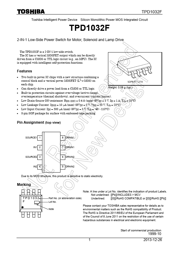
- 8-pin SOP package for surface with embossed-tape packing