TGA2597
Features
- Frequency Range: 2-6 GHz
- Output Power: > 31.5 d Bm (PIN = 18 d Bm)
- PAE: > 31 % (PIN = 18 d Bm)
- Large Signal Gain: > 13.5 d B (PIN = 18 d Bm)
- Small Signal Gain: > 24 d B
- VD = 25 V, IDQ = 40 m A, VG = -2.5 V typ.
- Chip Dimensions: 2.140 mm x 1.500 mm x 0.10 mm
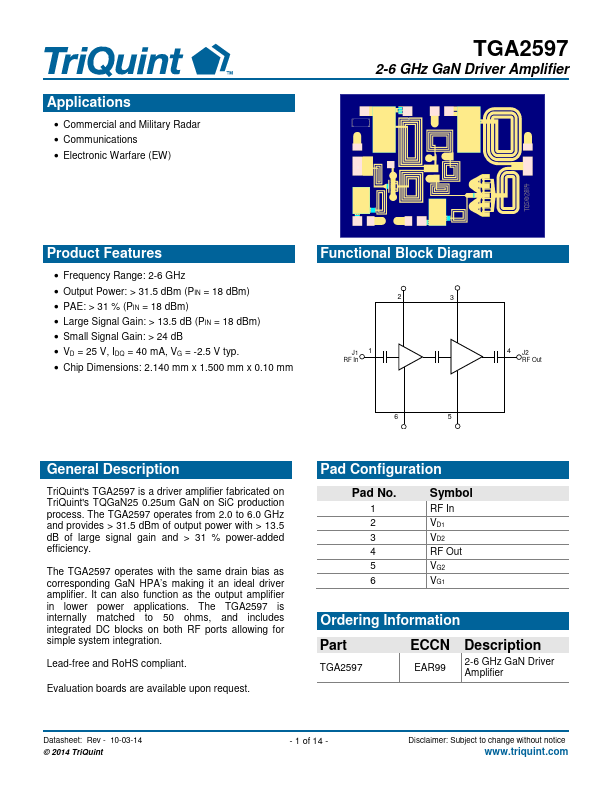
Functional Block Diagram
J1 1 RF In
4 J2 RF Out
General Description
Tri Quint's TGA2597 is a driver amplifier fabricated on Tri Quint's TQGa N25 0.25um Ga N on Si C production process. The TGA2597 operates from 2.0 to 6.0 GHz and provides > 31.5 d Bm of output power with > 13.5 d B of large signal gain and > 31 % power-added efficiency.
The TGA2597 operates with the same drain bias as corresponding Ga N HPA’s making it an ideal driver amplifier. It can also function as the output amplifier in lower power applications. The TGA2597 is internally matched to 50 ohms, and includes integrated DC blocks on both RF ports allowing for simple system integration.
Lead-free and Ro HS pliant.
Evaluation boards are available...