TQ1090
TQ1090 is 11-Output Configurable Clock Buffer manufactured by TriQuint Semiconductor.
S E M I C O N D U C T O R, I N C .
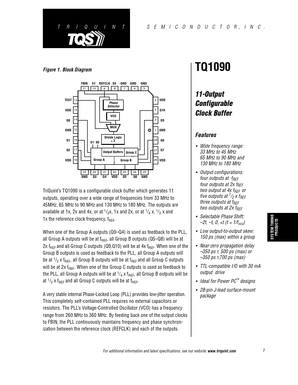
Figure 1. Block Diagram
FBIN
S1
REFCLK S0
9 8
TEST 12 VDD 13
Phase Detector VCO
4 VDD 3 2
Q10 Q9
11-Output Configurable Clock Buffer
Features
Q0
GND 15 Q1 Q2
16 17
MUX Divide Logic ÷2 Output Buffers Group C Group A Group B
1 GND 28 27
S1 S0
Q8 Q7
VDD 18
26 VDD
- Wide frequency range: 33 MHz to 45 MHz 65 MHz to 90 MHz and 130 MHz to 180 MHz
- Output configurations: four outputs at fREF four outputs at 2x fREF two output at 4x fREF or five outputs at 1/2 x fREF three outputs at fREF two outputs at 2x fREF
- Selectable Phase Shift:
- 2t,
- t, 0, +t (t = 1/fvco)
- Low output-to-output...