TSP630M Key Features
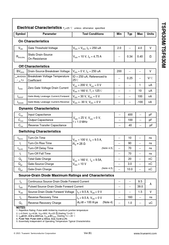
- 9.5A,200V,Max.RDS(on)=0.40 Ω @ VGS =10V
- Low gate charge(typical 20nC)
- High ruggedness
- Fast switching
- 100% avalanche tested
- Improved dv/dt capability
TSP630M is N-Channel MOSFET manufactured by Truesemi.
| Part Number | Description |
|---|---|
| TSP60R150WT | N-Channel MOSFET |
| TSP60R190S1 | N-Channel MOSFET |
| TSP60R280S1 | N-Channel MOSFET |
| TSP60R2K3S1 | N-Channel MOSFET |
| TSP60R380S1 | N-Channel MOSFET |
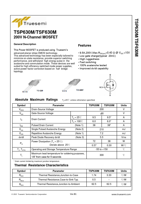
This Power MOSFET is produced using Truesemi‘s advanced planar stripe DMOS technology. This advanced technology has been especially tailored to minimize on-state resistance, provide superior switching performance, and withstand high energy pulse in the avalanche and mutation mode. These devices are well suited for high efficiency switched mode power supplies, active power factor correction based on half bridge...