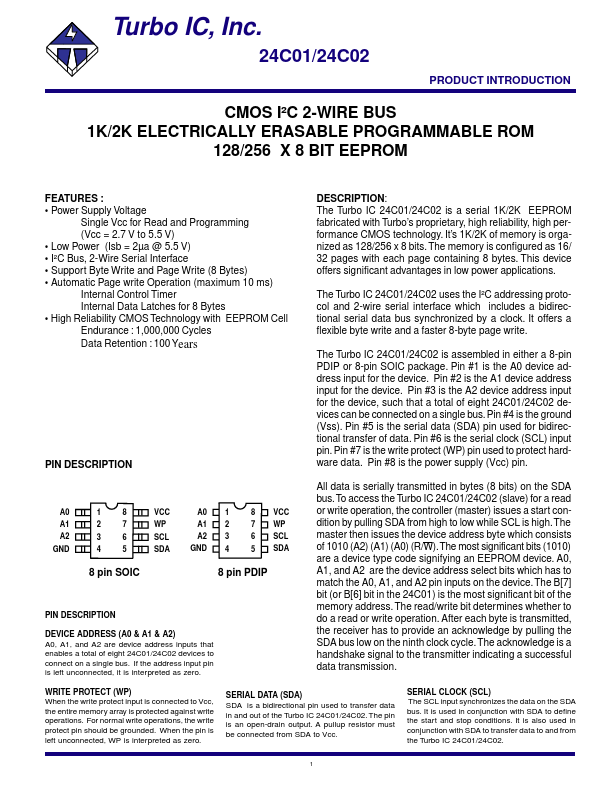
• Part: 24C01
  • Description: 1K/2K ELECTRICALLY ERASABLE PROGRAMMABLE ROM
  • Manufacturer: Turbo IC
  • Size: 46.73 KB
Download 24C01 Datasheet PDF
24C01 page 2
Page 2
24C01 page 3
Page 3

24C01 Datasheet Text

Turbo IC, Inc. 24C01/24C02 PRODUCT INTRODUCTION CMOS I²C 2-WIRE BUS 1K/2K ELECTRICALLY ERASABLE PROGRAMMABLE ROM 128/256 X 8 BIT EEPROM Features : - Power Supply Voltage Single Vcc for Read and Programming (Vcc = 2.7 V to 5.5 V) - Low Power (Isb = 2µa @ 5.5 V) - I²C Bus, 2-Wire Serial Interface - Support Byte Write and Page Write (8 Bytes) - Automatic Page write Operation (maximum 10 ms) Internal Control Timer Internal Data Latches for 8 Bytes - High Reliability CMOS Technology with EEPROM Cell Endurance : 1,000,000 Cycles Data Retention : 100 Years DESCRIPTION: The Turbo IC 24C01/24C02 is a serial 1K/2K EEPROM fabricated with Turbo’s proprietary, high reliability, high performance CMOS technology. It’s 1K/2K of memory is organized as 128/256 x 8 bits. The memory is configured as 16/ 32 pages with each page containing 8 bytes. This device offers significant advantages in low power applications. The Turbo IC 24C01/24C02 uses the I²C addressing protocol and 2-wire serial interface which includes a bidirectional serial data bus synchronized by a clock. It offers a flexible byte write and a faster 8-byte page write. The Turbo IC 24C01/24C02 is assembled in either a 8-pin PDIP or 8-pin SOIC package. Pin #1 is the A0 device address input for the device. Pin #2 is the A1 device address input for the device. Pin #3 is the A2 device address input for the device, such that a total of eight 24C01/24C02 devices can be connected on a single bus. Pin #4 is the ground (Vss). Pin #5 is the serial data (SDA) pin used for bidirectional transfer of data. Pin #6 is the serial clock (SCL) input pin. Pin #7 is the write protect (WP) pin used to protect hardware data. Pin #8 is the power supply (Vcc) pin. All data is serially transmitted in bytes (8 bits) on the SDA bus. To access the...