PE3 Overview
Description
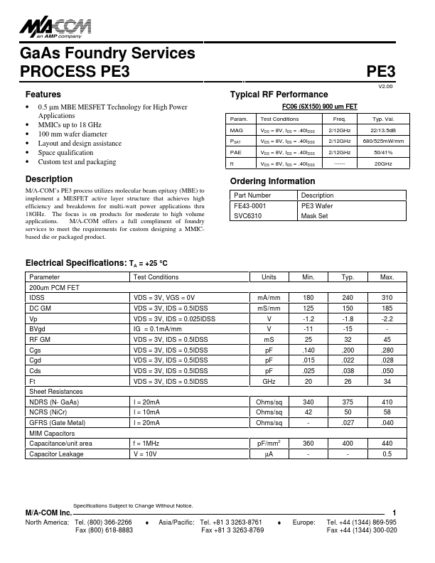
M/A-COM’s PE3 process utilizes molecular beam epitaxy (MBE) to implement a MESFET active layer structure that achieves high efficiency and breakdown for multi-watt power applications thru 18GHz. The focus is on products for moderate to high volume applications.
Key Features
- MAG PSAT PAE ft Test Conditions VDS = 8V, IDS = .40IDSS VDS = 8V, IDS = .40IDSS VDS = 8V, IDS = .40IDSS VDS = 8V, IDS = .40IDSS Freq
- 2/12GHz 2/12GHz 2/12GHz -----Typ
- 22/13.5dB 680/525mW/mm 50/41% 20GHz