Datasheet4U Logo Datasheet4U.com

NTMD3P03R2G Datasheet Dual -30v P-channei MOSFET

Manufacturer: UMW

Overview: UMW NTMD3P03R2G Dual -30V P-ChanneI MOSFET 1.

Datasheet Details

Part number NTMD3P03R2G
Manufacturer UMW
File Size 197.93 KB
Description Dual -30V P-ChanneI MOSFET
Datasheet NTMD3P03R2G-UMW.pdf

General Description

SOP-8 2,4 G GATE 1,3 5,6,7,8 S SOURCE D DRAIN G1 G2 S1 G1 S2 G2 1234 S1 S2 3.Absolute Maximum Ratings TJ=25°C unless otherwise noted Parameter Drain-Source Voltage Gate-Source Voltage Junction−to−Ambient (Note 1) Total Power Dissipation @ TA=25°C Continuous Drain Current @ 25°C Continuous Drain Current @ 70°C Pulsed Drain Current (Note 4) Junction−to−Ambient (Note 2) Total Power Dissipation @ TA=25°C Continuous Drain Current @ 25°C Continuous Drain Current @ 70°C Pulsed Drain Current (Note 4) Thermal Resistance Thermal Resistance Symbol VDSS VGSS RθJA PD ID ID IDM RθJA PD ID ID IDM Maximum Units -30 V ±20 V 171 °C/W 0.73 W -2.34 A -1.87 A -8 A 100 °C/W 1.25 W -3.05 A -2.44 A -12 A UTD Semiconductor Co.,Limited .umw-ic.

Nov.2024 1 of 10 .umw-ic.

UMW NTMD3P03R2G Dual -30V P-ChanneI MOSFET Junction−to−Ambient (Note 3) Total Power Dissipation @ TA=25°C Continuous Drain Current @ 25°C Thermal Resistance Continuous Drain Current @ 70°C Pulsed Drain Current (Note 4) Operating and StorageTemperature Range Single Pulse Drain−to−Source Avalanche Energy − Starting TJ=25°C (VDD=-30Vdc, VGS=−4.5Vdc, Peak IL=−7.5 Apk, L=5 mH, RG=25Ω) Maximum Lead Temperature for Soldering Purposes, 1/8” from case for 10 seconds RθJA PD ID ID IDM TJ, Tstg EAS TL 62.5 2 -3.86 -3.1 -15 -55 to 150
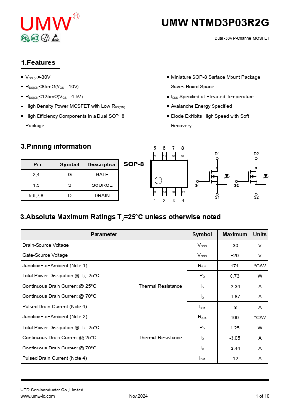
 °C/W W A A A °C 140 mJ 260 °C 2 of 10 UTD Semiconductor Co.,Limited Nov.2024 .umw-ic.

Key Features

  • VDS (V)=-30V RDS(ON).

NTMD3P03R2G Distributor