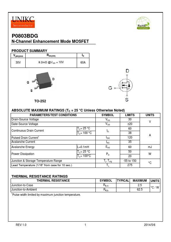
P0803BDG Overview
| Part | P0803BDG |
|---|---|
| Description | MOSFET |
| Category | MOSFET |
| Manufacturer | UNIKC |
| Size | 506.36 KB |
| Seller | Inventory | Price Breaks | Buy |
|---|---|---|---|
| UnikeyIC | 400000 | 100+ : 0.1511 USD 200+ : 0.1486 USD 300+ : 0.1448 USD |
View Offer |
| Unikeyic (ICkey) | 400000 | 100+ : 0.1511 USD 200+ : 0.1486 USD 300+ : 0.1448 USD |
View Offer |
| Part Number | Manufacturer | Description |
|---|---|---|
| CBR3A-P080 | Central Semiconductor | Bridge Rectifiers/ Controlled Avalanche |
| P0808ATG | NIKO-SEM | N-Channel Transistor |
| P0808ATG | VBsemi | N-Channel MOSFET |