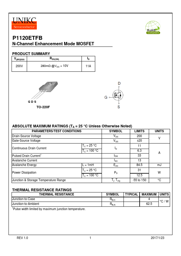
P1120ETFB
P1120EDB
P1120ETFB Datasheet (UNIKC)
Part
P1120ETFB
Description
N-Channel MOSFET
Category
MOSFET
Manufacturer
UNIKC
Size
775.62 KB
P1120ETFB Datasheet (PDF) Download
🏠
🔍
🌙
UNIKC
P1120ETFB Overview
Related Datasheets
Part Number
Manufacturer
Description
P1120ETFB
NIKO-SEM
N-Channel MOSFET
P1120ETFB Datasheet
🏠
🔍
This website uses cookies or similar technologies, to enhance your browsing experience and provide personalized recommendations.
By continuing to use our website, you agree to our
Privacy Policy
Accept