The following content is an automatically extracted verbatim text
from the original manufacturer datasheet and is provided for reference purposes only.
View original datasheet text
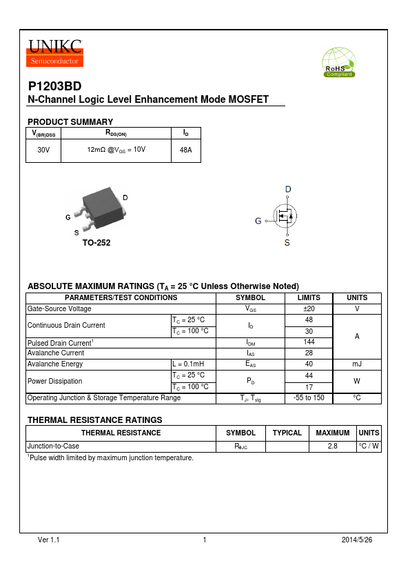
P1203BD
N-Channel Logic Level Enhancement Mode MOSFET
PRODUCT SUMMARY
V(BR)DSS
RDS(ON)
ID
30V
12mΩ @VGS = 10V
48A
TO-252
ABSOLUTE MAXIMUM RATINGS (TA = 25 °C Unless Otherwise Noted)
PARAMETERS/TEST CONDITIONS
SYMBOL
LIMITS
Gate-Source Voltage
VGS
±20
Continuous Drain Current Pulsed Drain Current1
TC = 25 °C
ID
48
TC = 100 °C
30
IDM
144
Avalanche Current
IAS
28
Avalanche Energy
L = 0.1mH
EAS
40
Power Dissipation
TC = 25 °C
PD
44
TC = 100 °C
17
Operating Junction & Storage Temperature Range
TJ, Tstg
-55 to 150
UNITS V
A
mJ W °C
THERMAL RESISTANCE RATINGS
THERMAL RESISTANCE Junction-to-Case 1Pulse width limited by maximum junction temperature.
SYMBOL RqJC
TYPICAL
MAXIMUM UNITS
2.8
°C / W
Ver 1.