P3503EVG
Description
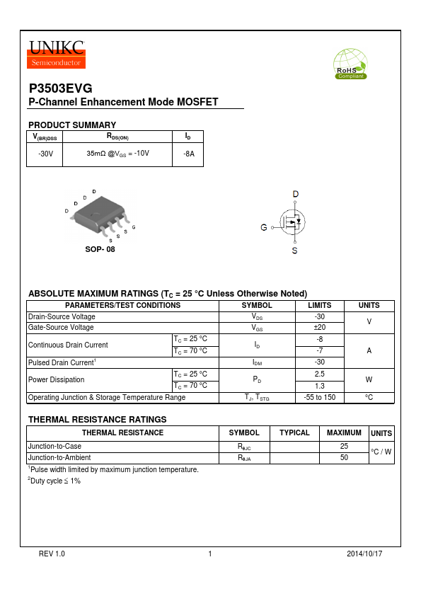
P3503EVG P-Channel Enhancement Mode MOSFET PRODUCT SUMMARY V(BR)DSS RDS(ON) -30V 35mΩ @VGS = -10V ID -8A SOP- 08 ABSOLUTE MAXIMUM RATINGS (TC = 25 °C Unless Otherwise Noted) PARAMETERS/TEST C...
P3503EVG P-Channel Enhancement Mode MOSFET PRODUCT SUMMARY V(BR)DSS RDS(ON) -30V 35mΩ @VGS = -10V ID -8A SOP- 08 ABSOLUTE MAXIMUM RATINGS (TC = 25 °C Unless Otherwise Noted) PARAMETERS/TEST C...