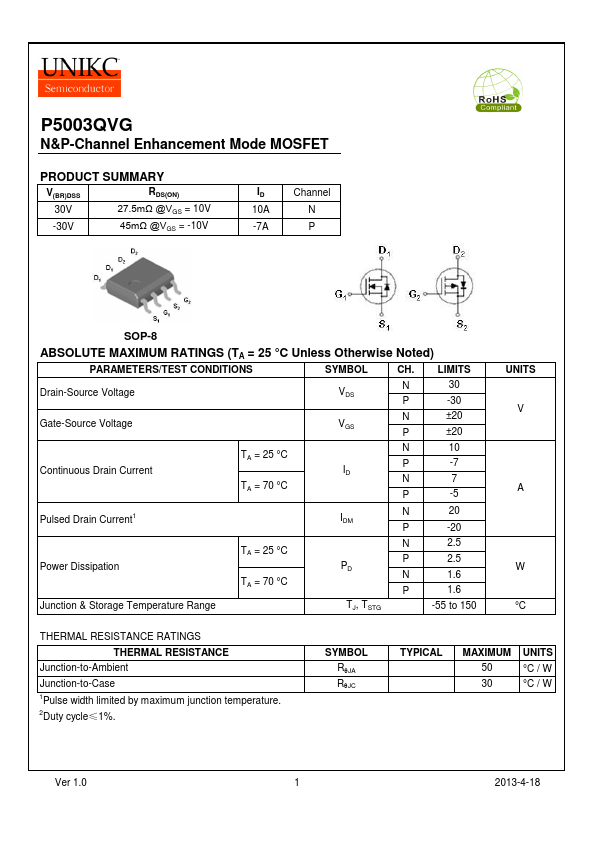
P5003QVG
Key Features
- V(BR)DSS, VGS = 10V
- V(BR)DSS, VGS = -10V, N
Representative P5003QVG image (package may vary by manufacturer)
Representative P5003QVG image (package may vary by manufacturer)
| Part Number | Manufacturer | Description |
|---|---|---|
| P5003QVG | NIKO-SEM | N&P-Channel MOSFET |
| PDV-P5003 | Advanced Photonix | CdS Photoconductive Photocells |
| P5000SB | Kexin Semiconductor | Thyristor Surge Suppressors |
| P500HVN01.0 | AU Optronics | TFT LCD Module |
| P500HVF01.0 | AU Optronics | TFT LCD Module |
| P5000SB | SOCAY | Thyristor Surge Suppressors |
| PDV-P5001 | Advanced Photonix | CdS Photoconductive Photocells |
| PDV-P5002 | Advanced Photonix | CdS Photoconductive Photocells |
| P5000MC | WPM | Thyristors Solid Protection Device Bidirectional transient voltage suppressors |
| P5000SC | WPM | Thyristors Solid Protection Device Bidirectional transient voltage suppressors |