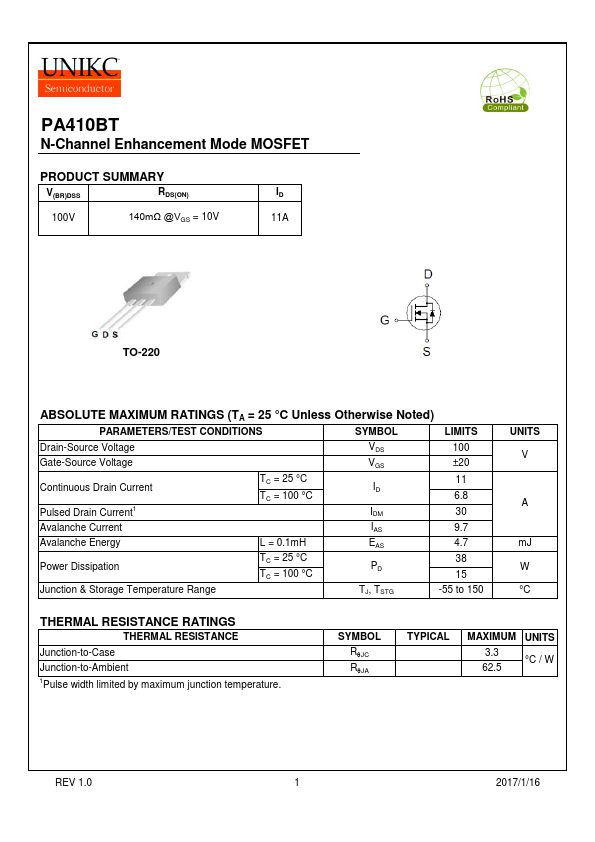
Click to expand full text
PA410BT
N-Channel Enhancement Mode MOSFET
PRODUCT SUMMARY
V(BR)DSS
RDS(ON)
ID
100V
140mΩ @VGS = 10V
11A
TO-220
ABSOLUTE MAXIMUM RATINGS (TA = 25 °C Unless Otherwise Noted)
PARAMETERS/TEST CONDITIONS
SYMBOL
LIMITS
Drain-Source Voltage
VDS
100
Gate-Source Voltage
VGS
±20
Continuous Drain Current Pulsed Drain Current1
TC = 25 °C TC = 100 °C
ID
11 6.8
IDM
30
Avalanche Current
IAS
9.7
Avalanche Energy
L = 0.1mH
EAS
4.7
Power Dissipation
TC = 25 °C TC = 100 °C
PD
38 15
Junction & Storage Temperature Range
TJ, TSTG
-55 to 150
UNITS V
A
mJ W °C
THERMAL RESISTANCE RATINGS
THERMAL RESISTANCE Junction-to-Case Junction-to-Ambient 1Pulse width limited by maximum junction temperature.
SYMBOL RqJC RqJA
TYPICAL
MAXIMUM UNITS 3.3 °C / W 62.5
REV 1.