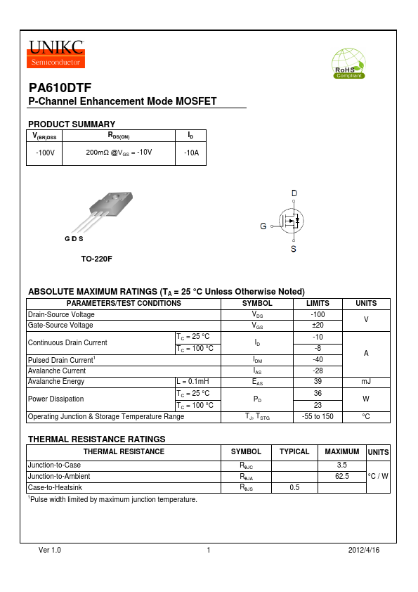
PA610DTF Overview
Key Features
- 2.0 -3.2 -4.0
| Part | PA610DTF |
|---|---|
| Description | P-Channel MOSFET |
| Category | MOSFET |
| Manufacturer | UNIKC |
| Size | 346.70 KB |
| Part Number | Manufacturer | Description |
|---|---|---|
| PA610AD | NIKO-SEM | N-Channel Transistor |
| PA6112 | Unisonic Technologies | DUAL 150MW AUDIO POWER AMPLIFIER |
| PA61 | APEX | Power Operational Amplifiers |
| PA61A | APEX | Power Operational Amplifiers |