DESCRIPTION
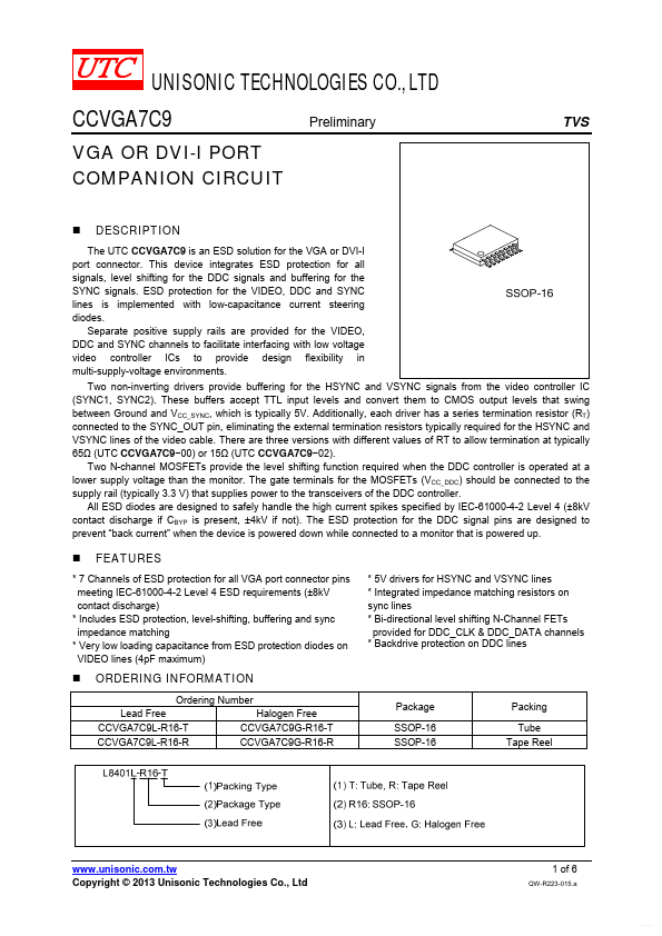
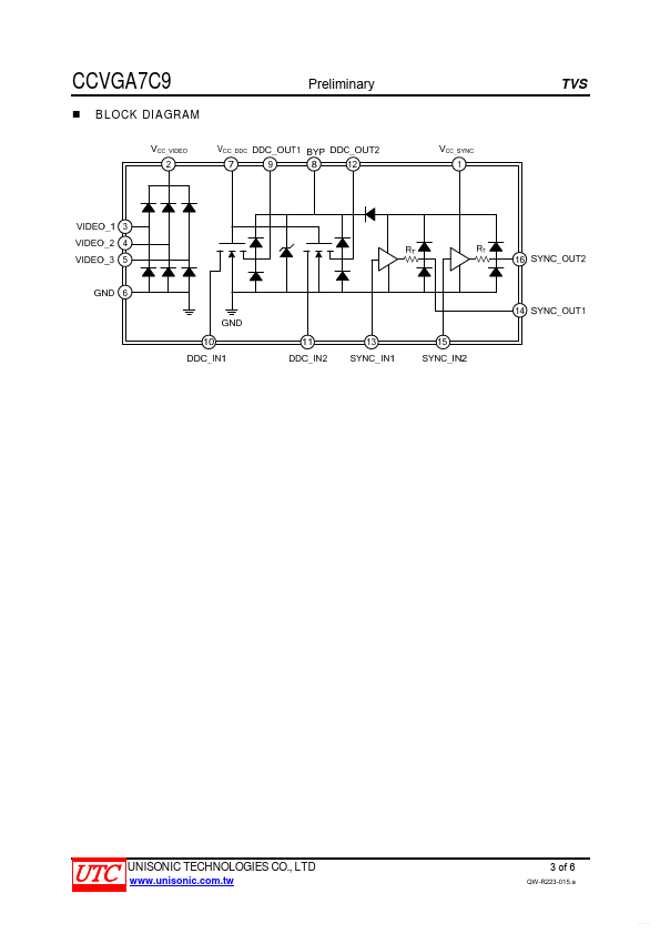
Preliminary TVS The UTC ESD protection for the VIDEO, DDC and SYNC lines is implemented with low-capacitance current steering diodes. Separate positive supply rails are provided for the VIDEO, DDC and SYNC channels to facilitate interfacing with low voltage video controller ICs to provide design flexibility in multi-supply-voltage environments. Two non-inverting drivers provide buffering for the HSYNC and VSYNC signals from the video controller IC (SYNC1, SYNC2). These buffers accept TTL input levels and convert them to CMOS output levels that swing between Ground and VCC_SYNC, which is typically 5V. Additionally, each driver has a series termination resistor (RT) connected to the SYNC_OUT pin, eliminating the external termination resistors typically required for the HSYNC and VSYNC lines of the video cable. There are three versions with different values of RT to allow termination at typically 65Ω (UTC CCVGA7C9−00) or 15Ω (UTC CCVGA7C9−02). Two N-channel MOSFETs provide the level shifting function required when the DDC controller is operated at a lower supply voltage than the monitor. Unisonic Technologies