Unisonic Technologies J113
J113 is designed for low level analog switching, sample and hold circuits and chopper stabilized amplifiers.| Part No. | J113 |
|---|---|
| Datasheet | J113 Download |
| Manufacturer |  Unisonic Technologies |
| Description | N-CHANNEL SWITCH |
| Buy | Stock & Price |

DESCRIPTION
The UTC●
FEATURES
* Source & Drain are interchangeable.● ORDERING INFORMATION Ordering Number Lead Free Halogen Free J113L-AE3-R J113G-AE3-R J113L-AE3-A-R J113G-AE3-A-R Note: Pin Assignment: D: Drain S: Source G: Gate Package SOT-23 SOT-23 Pin Assignment 1 2 3 D S G S D G Packing Tape Reel Tape Reel
● MARKING J113 J113-A Copyright © 2022 Unisonic Technologies Co., Ltd 1 of 4 QW-R228-003.D J113 N-CHANNEL JFET
●
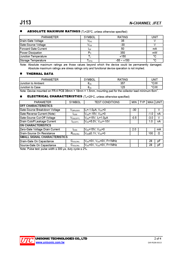
ABSOLUTE MAXIMUM RATINGS
(TA=25°С, unless otherwise specified) PARAMETER SYMBOL RATING UNIT Drain-Gate Voltage VDG 35 V Gate-Source Voltage VGS -30 V Forward Gate Current IGF 50 mA Power Dissipation PD 350 mW Junction Temperature TJ +150 °С Storage Temperature TSTG -55 ~ +150 °С Note: Absolute maximum ratings are those values beyond which the device could be permanently damaged. Absolute maximum ratings are stress ratings only and functional device operation is not implied.● THERMAL DATA PARAMETER SYMBOL RATING UNIT Junction to Ambient θJA 357 °C/W Junction to Case θJC 125 °C/W Note: Device mounted on FR-4 PCB 36mm × 18mm × 1.5mm, mounting pad for the collector lead minimum 6cm2.