Datasheet4U Logo Datasheet4U.com

CHA3511-99F - Amplifier

Datasheet Summary

Description

by a double stage travelling wave amplifier.

applications.

both RF and DC grounded.

Features

  • Wide Band: 6-18GHz.
  • 16dB gain.
  • 39dB isolation.
  • 22 dBm saturated output power.
  • DC power consumption, 190mA @ 4.5V.
  • Chip size: 3.55 x 2.30 x 0.1mm dBS21 (dB) 30 20 10 0 -10 -20 -30 -40 -50 -60 2 4 6 8 10 12 14 16 18 20 Frequency GHz Typical on wafer Measurements Gain versus switch states Main Characteristics Tamb. = 25°C Symbol Parameter Fop Operating frequency range Min Typ Max Unit 6 18 GHz G Small signal gain @ Switch on 15 16 dB.

📥 Download Datasheet

Datasheet preview – CHA3511-99F

Datasheet Details

Part number CHA3511-99F
Manufacturer United Monolithic Semiconductors
File Size 654.14 KB
Description Amplifier
Datasheet download datasheet CHA3511-99F Datasheet
Additional preview pages of the CHA3511-99F datasheet.
Other Datasheets by United Monolithic Semiconductors

Full PDF Text Transcription

Click to expand full text
CHA3511-99F 6-18GHz Amplifier GaAs Monolithic Microwave IC Description 
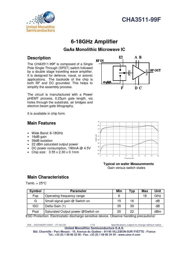
E2 RF IN The CHA3511-99F is composed of a Single Pole Single Through (SPST) switch followed by a double stage travelling wave amplifier. It is designed for defence, naval, or avionic applications. The backside of the chip is both RF and DC grounded. This helps to simplify the assembly process. F The circuit is manufactured with a Power pHEMT process, 0.25µm gate length, via holes through the substrate, air bridges and electron beam gate lithography. It is available in chip form. AB RF OUT DC Main Features  Wide Band: 6-18GHz  16dB gain  39dB isolation  22 dBm saturated output power  DC power consumption, 190mA @ 4.5V  Chip size: 3.55 x 2.30 x 0.
Published: |