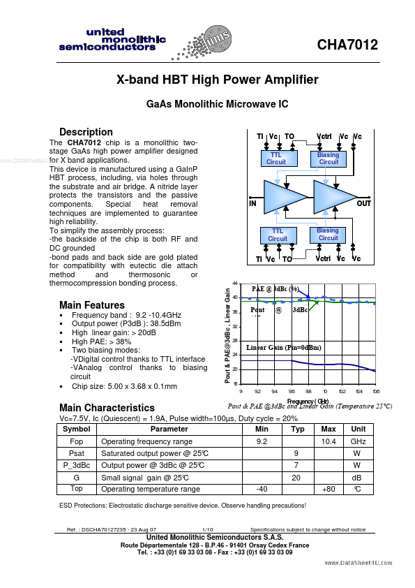
Datasheet4U Logo Datasheet4U.com

CHA7012 - X-band HBT High Power Amplifier

Datasheet Summary

Description

The CHA7012 chip is a monolithic twostage GaAs high power amplifier designed www.DataSheet4U.com for X band applications.

This device is manufactured using a GaInP HBT process, including, via holes through the substrate and air bridge.

Features

  • Frequency band : 9.2 -10.4GHz Output power (P3dB ): 38.5dBm High linear gain: > 20dB High PAE: > 38% Two biasing modes: -VDigital control thanks to TTL interface -VAnalog control thanks to biasing circuit Chip size: 5.00 x 3.68 x 0.1mm Pout (dBm @ 3dBc Linear Gain (Pin=0dBm) 24 20 1 6 9 9.2 9.4 9.6 9.8 1 0 1 0.2 1 0.4 1 0.6 Main Characteristics Pout & PAE @3dBc and Linear Gain (Temperature 25°C) Frequency ( G H z) Vc=7.5V, Ic (Quiescent) = 1.9A, Pulse width=100µs, Duty cycle = 20% Symbol.

📥 Download Datasheet

Datasheet preview – CHA7012

Datasheet Details

Part number CHA7012
Manufacturer United Monolithic Semiconductors
File Size 604.20 KB
Description X-band HBT High Power Amplifier
Datasheet download datasheet CHA7012 Datasheet
Additional preview pages of the CHA7012 datasheet.
Other Datasheets by United Monolithic Semiconductors

Full PDF Text Transcription

Click to expand full text
CHA7012 X-band HBT High Power Amplifier GaAs Monolithic Microwave IC Description The CHA7012 chip is a monolithic twostage GaAs high power amplifier designed www.DataSheet4U.com for X band applications. This device is manufactured using a GaInP HBT process, including, via holes through the substrate and air bridge. A nitride layer protects the transistors and the passive components. Special heat removal techniques are implemented to guarantee high reliability. To simplify the assembly process: -the backside of the chip is both RF and DC grounded -bond pads and back side are gold plated for compatibility with eutectic die attach method and thermosonic or thermocompression bonding process.
Published: |