Datasheet4U Logo Datasheet4U.com

CHKA012a99F - 140W Power Bar

Datasheet Summary

Description

The CHKA012a99F is a 140W Gallium Nitride High Electron Mobility Transistor.

This product offers a general purpose and broadband solution for a variety of RF power applications such as radar and telecommunication.

Features

  • Wide band capability up to 4GHz.
  • Pulsed and CW operating modes.
  • GaN technology: High Pout & High PAE.
  • DC bias: VDS up to 50V.
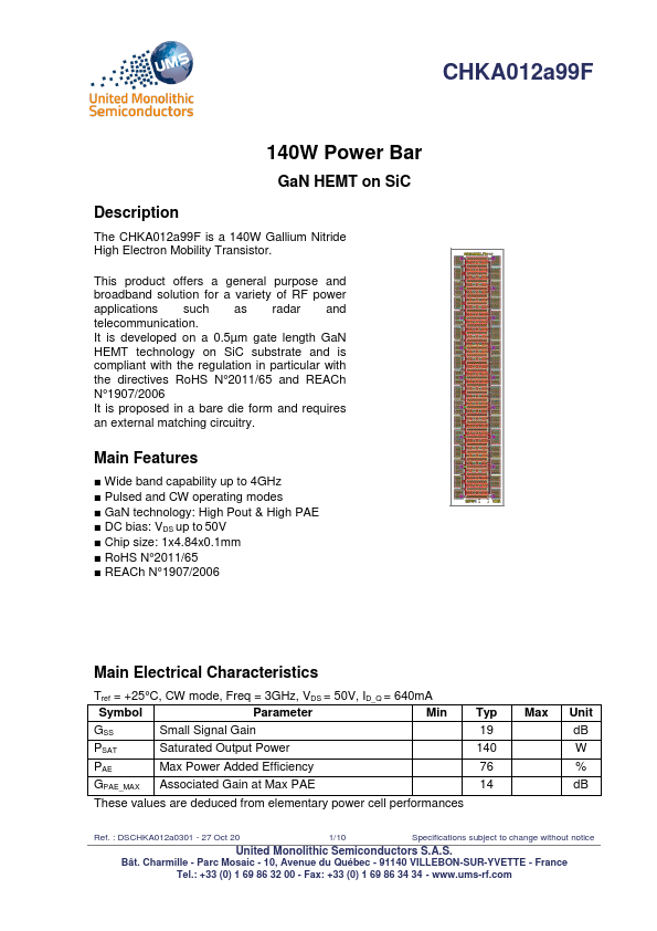
  • Chip size: 1x4.84x0.1mm.
  • RoHS N°2011/65.
  • REACh N°1907/2006 Main Electrical Characteristics Tref = +25°C, CW mode, Freq = 3GHz, VDS = 50V, ID_Q = 640mA Symbol Parameter Min Typ GSS Small Signal Gain 19 PSAT Saturated Output Power 140 PAE Max Power Added Efficiency 76 GPAE_MAX Associated Gain at Max PAE 14 These values ar.

📥 Download Datasheet

Datasheet preview – CHKA012a99F

Datasheet Details

Part number CHKA012a99F
Manufacturer United Monolithic Semiconductors
File Size 516.05 KB
Description 140W Power Bar
Datasheet download datasheet CHKA012a99F Datasheet
Additional preview pages of the CHKA012a99F datasheet.
Other Datasheets by United Monolithic Semiconductors

Full PDF Text Transcription

Click to expand full text
CHKA012a99F 140W Power Bar GaN HEMT on SiC Description The CHKA012a99F is a 140W Gallium Nitride High Electron Mobility Transistor. This product offers a general purpose and broadband solution for a variety of RF power applications such as radar and telecommunication. It is developed on a 0.5µm gate length GaN HEMT technology on SiC substrate and is compliant with the regulation in particular with the directives RoHS N°2011/65 and REACh N°1907/2006 It is proposed in a bare die form and requires an external matching circuitry. Main Features ■ Wide band capability up to 4GHz ■ Pulsed and CW operating modes ■ GaN technology: High Pout & High PAE ■ DC bias: VDS up to 50V ■ Chip size: 1x4.84x0.
Published: |