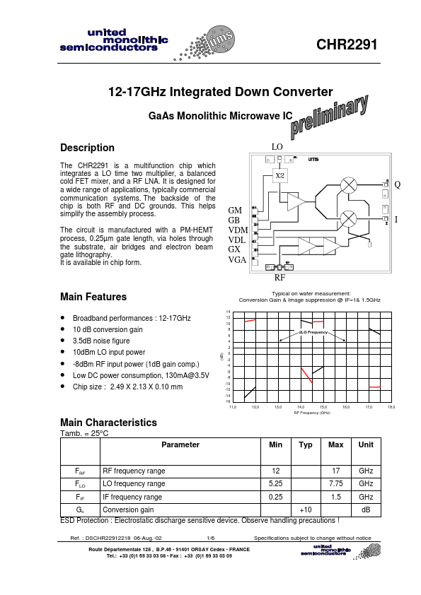
Datasheet4U Logo Datasheet4U.com

CHR2291 - 12-17GHz Integrated Down Converter

Datasheet Summary

Description

The CHR2291 is a multifunction chip which integrates a LO time two multiplier, a balanced cold FET mixer, and a RF LNA.

It is designed for a wide range of applications, typically commercial communication systems.

The backside of the chip is both RF and DC grounds.

Features

  • 14 Typical on wafer measurement: Conversion Gain & Image suppression @ IF=1& 1.5GHz 12 10 8 6 4 2 0 -2 -4 -6 -8 -10 -12 -14 -16 11,0 12,0 13,0 14,0 15,0 16,0 17,0 18,0 Broadband performances : 12-17GHz 10 dB conversion gain 3.5dB noise figure -8dBm RF input power (1dB gain comp. ) Low DC power consumption, 130mA@3.5V Chip size : 2.49 X 2.13 X 0.10 mm (dB) 2LO Frequency 10dBm LO input power RF Frequency (GHz) Main Characte.

📥 Download Datasheet

Datasheet preview – CHR2291

Datasheet Details

Part number CHR2291
Manufacturer United Monolithic Semiconductors
File Size 121.33 KB
Description 12-17GHz Integrated Down Converter
Datasheet download datasheet CHR2291 Datasheet
Additional preview pages of the CHR2291 datasheet.
Other Datasheets by United Monolithic Semiconductors

Full PDF Text Transcription

Click to expand full text
CHR2291 12-17GHz Integrated Down Converter GaAs Monolithic Microwave IC Description The CHR2291 is a multifunction chip which integrates a LO time two multiplier, a balanced cold FET mixer, and a RF LNA. It is designed for a wide range of applications, typically commercial communication systems. The backside of the chip is both RF and DC grounds. This helps simplify the assembly process. The circuit is manufactured with a PM-HEMT process, 0.25µm gate length, via holes through the substrate, air bridges and electron beam gate lithography. It is available in chip form. LO Q GM GB VDM VDL GX VGA RF I Main Features • • • • • • • 14 Typical on wafer measurement: Conversion Gain & Image suppression @ IF=1& 1.
Published: |