CHX2089 Overview
Key Features
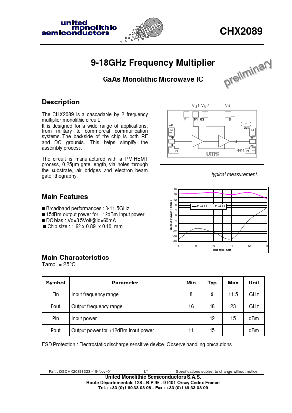
- Broadband performances : 8-11.5GHz
- 15dBm output power for +12dBm input power
- DC bias : Vd=3.5Volt@Id=60mA
| Part | CHX2089 |
|---|---|
| Description | 9-18GHz Frequency Multiplier |
| Manufacturer | United Monolithic Semiconductors |
| Size | 77.38 KB |
| Seller | Inventory | Price Breaks | Buy |
|---|---|---|---|
| Walker Industrial | -4 | 1+ : 684.3 USD | View Offer |
| RS (Formerly Allied Electronics) | 0 | 1+ : 900.63 USD | View Offer |
| Part Number | Manufacturer | Description |
|---|---|---|
| AD835 | Analog Devices | 4-Quadrant Multiplier |
| AD734 | Analog Devices | 10 MHz/ 4-Quadrant Multiplier/Divider |
| HA1-2556883 | Intersil | Wideband Four Quadrant Analog Multiplier (Voltage Output) |