CHX2193-FAB Overview
Description
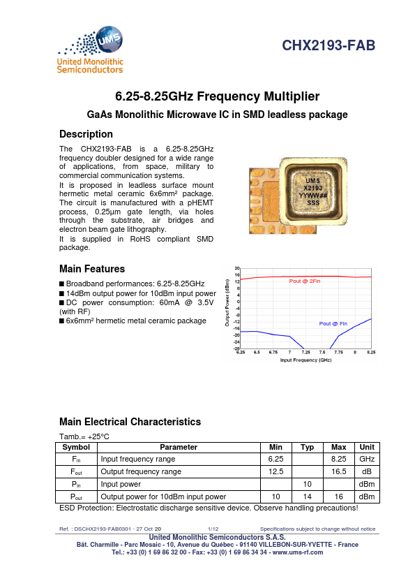
The CHX2193-FAB is a 6.25-8.25GHz frequency doubler designed for a wide range of applications, from space, military to commercial communication systems. It is proposed in leadless surface mount hermetic metal ceramic 6x6mm² package.
Key Features
- Broadband performances: 6.25-8.25GHz
- 14dBm output power for 10dBm input power
- DC power consumption: 60mA @ 3.5V (with RF)
- 10, Avenue du Québec
- 91140 VILLEBON-SUR-YVETTE