HY4903B Key Features
- Halogen-free According to IEC 61249-2-21
- Trench Power MOSFET
- Package with Low Thermal Resistance
- 100 % Rg and UIS Tested
- pliant to RoHS Directive 2002/95/EC
HY4903B is N-Channel 30V MOSFET manufactured by VBsemi.
| Manufacturer | Part Number | Description |
|---|---|---|
| HY4903B | N-Channel MOSFET | |
| HY4903B6 | N-Channel Enhancement Mode MOSFET | |
| HY4903P | N-Channel MOSFET |
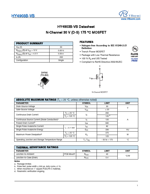
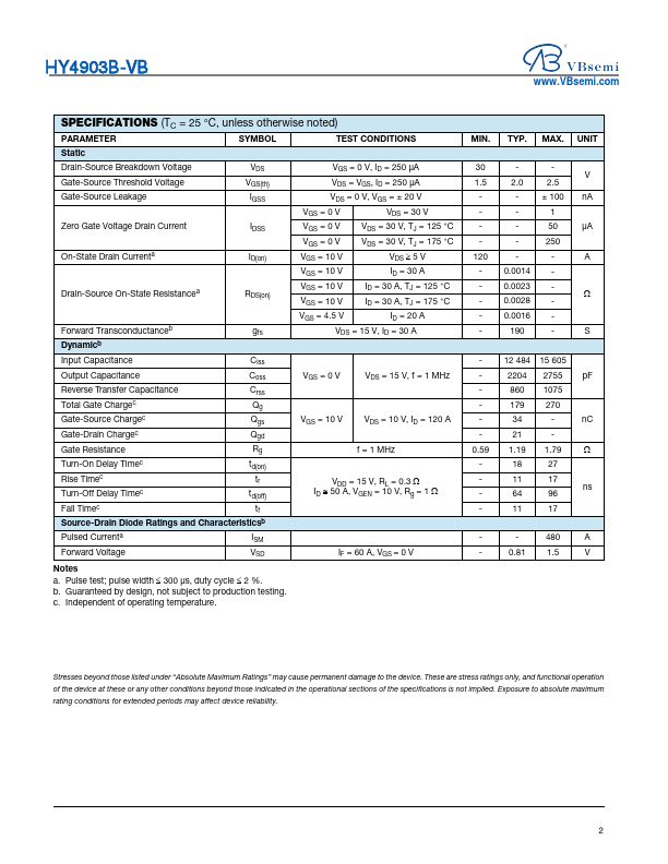
HY4903B-VB HY4903B-VB Datasheet N-Channel 30 V (D-S) 175 °C MOSFET .VBsemi. PRODUCT SUMMARY VDS (V) RDS(on) () at VGS = 10 V RDS(on) () at VGS = 4.5 V ID (A) Configuration 30 0.0014 0.0016 260 Single D2PAK (TO-263) G D.