FCSP0530ETR Overview
Key Specifications
Mount Type: Surface Mount
Max Operating Temp: 150 °C
Min Operating Temp: -55 °C
Description
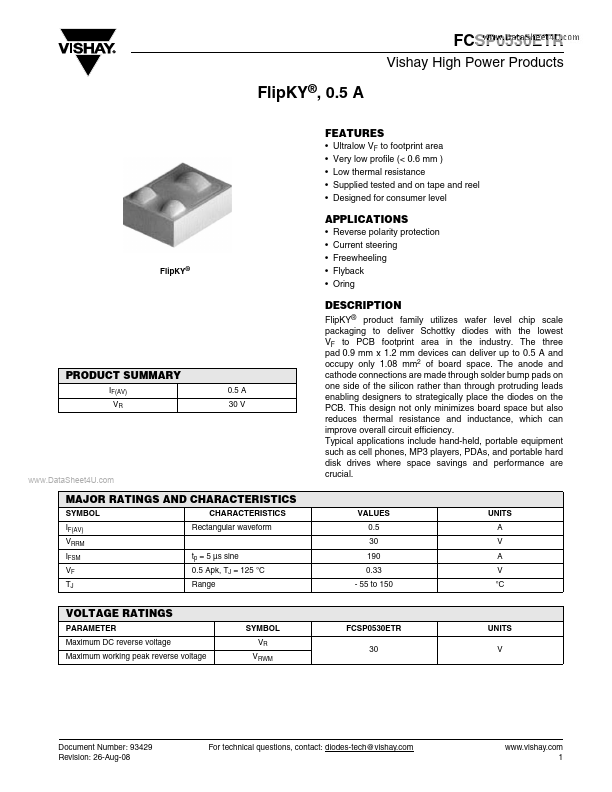
FlipKY® product family utilizes wafer level chip scale packaging to deliver Schottky diodes with the lowest VF to PCB footprint area in the industry. The three pad 0.9 mm x 1.2 mm devices can deliver up to 0.5 A and occupy only 1.08 mm2 of board space.
Key Features
- Ultralow VF to footprint area Very low profile (< 0.6 mm ) Low