SI4726CY
SI4726CY is N-Channel MOSFET manufactured by Vishay.
FEATURES
D D D D 4.5- to 20-V Operation Driver Impedance- 3 W Undervoltage Lockout Fast Switching Times (30 ns typ.) D D D D 20-V MOSFETs High Side: 0.0135 W @ VDD = 4.5 V Low Side: 0.0065 W @ VDD = 4.5 V Switching Frequency: 250 k Hz to 1 MHz
DESCRIPTION
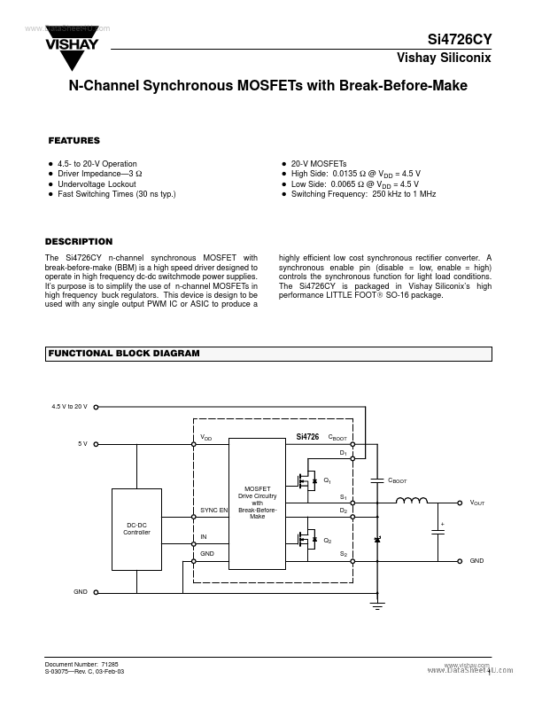
The Si4726CY n-channel synchronous MOSFET with break-before-make (BBM) is a high speed driver designed to operate in high frequency dc-dc switchmode power supplies. It’s purpose is to simplify the use of n-channel MOSFETs in high frequency buck regulators. This device is design to be used with any single output PWM IC or ASIC to produce a highly efficient low cost synchronous rectifier converter. A synchronous enable pin (disable = low, enable = high) controls the synchronous function for light load conditions. The Si4726CY is packaged in Vishay Siliconix’s high performance LITTLE FOOTR SO-16 package.
FUNCTIONAL BLOCK DIAGRAM
4.5 V to 20 V
5V
Si4726
CBOOT D1
Q1 MOSFET Drive Circuitry with Break-Before Make S1 D2
CBOOT VOUT +
SYNC EN DC-DC Controller
IN GND
Q2 S2 GND
Document Number: 71285 S-03075- Rev. C, 03-Feb-03
.vishay.
..
Vishay Siliconix
ABSOLUTE MAXIMUM RATINGS (TA = 25_C UNLESS OTHERWISE NOTED)
Parameter
Logic Supply Logic Inputs Drain-Source Voltage Bootstrap Voltage Synchronous Pin Voltage Maximum Power Dissipationa Driver Operating Junction and Storage Temperature Range MOSFETs Tj, Tstg
Symbol
VDD VIN VDS VBOOT VSYNC PD
Steady State
7 -0.7 to VDD + 0.3 -1.0 to 20 7 -0.7 to VDD +0.3 4 -65 to 125 -65 to 150
Unit
W _C
Notes a. Surface mounted on 1” x1” FR4 board, full copper two sides. b. Pulse test: pulse width v300 m S, duty cycle v2%. Stresses beyond those listed under “Absolute Maximum Ratings” may cause permanent damage to the device. These are stress ratings only, and functional operation of the device at these or any other conditions beyond those indicated in the operational sections of the specifications is not implied. Exposure to absolute maximum rating...