SI4947DY Overview
Key Specifications
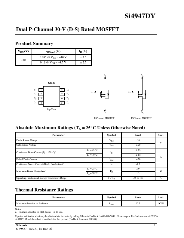
Package: SO
Pins: 8
Height: 1.55 mm
Length: 5 mm
Key Features
- 10 V 0.19 @ VGS =
- 30 "20 "3.5 "2.8 "20
Package: SO
Pins: 8
Height: 1.55 mm
Length: 5 mm
| Seller | Inventory | Price Breaks | Buy |
|---|---|---|---|
| Win Source | 7500 | 90+ : 0.6537 USD 220+ : 0.5359 USD 335+ : 0.5198 USD 460+ : 0.5024 USD |
View Offer |
| Best Source | 788 | 1+ : 0.4026 USD | View Offer |
| Part Number | Manufacturer | Description |
|---|---|---|
| SI4946DY | Kexin Semiconductor | Dual N-Channel MOSFET |
| SI4946DY-T1-E3 | VBsemi | 60V Dual N-Channel MOSFET |
| SI4946BEY-T1 | VBsemi | Dual N-Channel MOSFET |
| SI4946BEY-T1-E3 | VBsemi | Dual N-Channel MOSFET |
| Si4943CDY | Vishay | Dual P-Channel 20-V (D-S) MOSFET |