SI6866BDQ
SI6866BDQ is Dual N-Channel MOSFET manufactured by Vishay.
DESCRIPTION
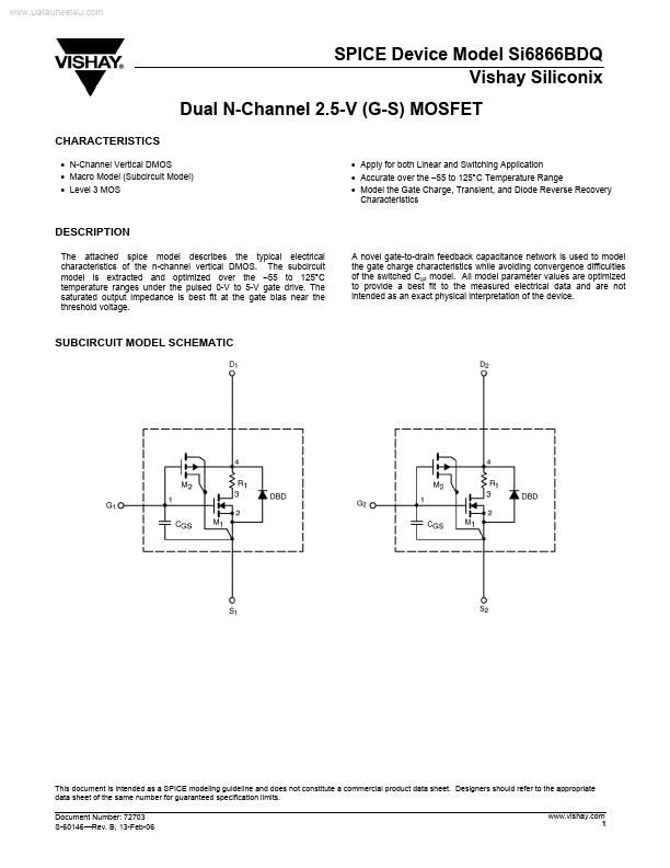
The attached spice model describes the typical electrical characteristics of the n-channel vertical DMOS. The subcircuit model is extracted and optimized over the
- 55 to 125°C temperature ranges under the pulsed 0-V to 5-V gate drive. The saturated output impedance is best fit at the gate bias near the threshold voltage. A novel gate-to-drain feedback capacitance network is used to model the gate charge characteristics while avoiding convergence difficulties of the switched Cgd model. All model parameter values are optimized to provide a best fit to the measured electrical data and are not intended as an exact physical interpretation of the device.
SUBCIRCUIT MODEL SCHEMATIC
This document is intended as a SPICE modeling guideline and does not constitute a mercial product data sheet. Designers should refer to the appropriate data sheet of the same number for guaranteed specification limits. Document Number: 72703 S-60146Rev. B, 13-Feb-06 .vishay. 1
SPICE Device Model Si6866BDQ Vishay Siliconix
SPECIFICATIONS (TJ = 25°C UNLESS OTHERWISE NOTED) Parameter Static
Gate Threshold Voltage On-State Drain Current a
Symbol
Test Condition
Simulated Data
1.1 115 0.020 0.032 21 0.80
Measured Data
Unit
VGS(th) ID(on) r DS(on) gfs VSD
VDS = VGS, ID = 250 µA VDS = 5 V, VGS = 4.5 V VGS = 4.5 V, ID = 6 A VGS = 2.5 V, ID = 4.9 A VDS = 10 V, ID = 6 A IS = 1.5 A, VGS = 0 V
V A 0.022 0.033 25 0.75 V Ω
Drain-Source On-State Resistancea Forward Transconductancea Forward Voltagea b
Dynamic
Total Gate Charge Gate-Source Charge Gate-Drain Charge Turn-On Delay Time Rise Time Turn-Off Delay Time Fall Time
Qg Qgs Qgd td(on) tr td(off) tf VDD = 10 V, RL = 10 Ω ID ≅ 1 A, VGEN = 4.5 V, RG = 6 Ω VDS = 10 V, VGS = 4.5 V, ID = 6 A
7.2 1.4 2.2 26 38 30 10
7.5 1.4 2.2 45 53 30 13 ns n C
Notes a. Pulse test; pulse width ≤ 300 µs, duty cycle ≤ 2%. b. Guaranteed by design, not subject to production testing.
.vishay. 2
Document Number: 72703 S-60146Rev. B, 13-Feb-06
SPICE...