VCR4N
FEATURES
D Continuous Voltage-Controlled Resistance D High Off-Isolation D High Input Impedance
BENEFITS
D Gain Ranging Capability/Wide Range Signal Attenuation D No Circuit Interaction D Simplified Drive
APPLICATIONS
D Variable Gain Amplifiers D Voltage Controlled Oscillator D AGC
DESCRIPTION
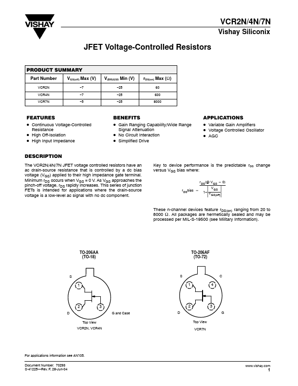
The VCR2N/4N/7N JFET voltage controlled resistors have an ac drain-source resistance that is controlled by a dc bias voltage (VGS) applied to their high impedance gate terminal. Minimum r DS occurs when VGS = 0 V. As VGS approaches the pinch-off voltage, r DS rapidly increases. This series of junction FETs is intended for applications where the drain-source voltage is a low-level ac signal with no dc ponent. Key to device performance is the predictable r DS change versus VGS bias where: r DS(@ V GS + 0) r DSbias [ V GS 1- V GS(off)
Ť Ť
These n-channel devices feature r DS(on) ranging from 20 to 8000 W . All packages are hermetically sealed and may be processed per MIL-S-19500 (see Military...