FEATURES
D D D D D D Monolithic Design High Slew Rate Low Offset/Drift Voltage Low Gate Leakage: 5 pA Low Noise High CMRR: 100 dB BENEFITS D Tight Differential Match vs. Current D Improved Op Amp Speed, Settling Time Accuracy D Minimum Input Error/Trimming Requirement D Insignificant Signal Loss/Error Voltage D High System Sensitivity D Minimum Error with Large Input Signal APPLICATIONS
D Wideband Differential Amps D High-Speed, Temp-Compensated, Single-Ended Input Amps D High Speed Comparators D Impedance Converters DESCRIPTION
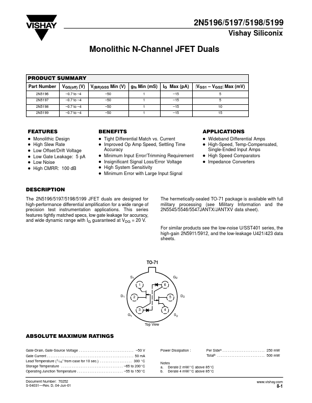
For similar products see the low-noise U/SST401 series, the high-gain 2N5911/5912, and the low-leakage U421/423 data sheets. TO-71 S1 1 D1 6 G2 2 5 D2 3 G1 Top View 4 S2 ABSOLUTE MAXIMUM RATINGS
Gate-Drain, Gate-Source Voltage . . . . . . . . . . . . . . . . . . . . . . . . . . . . . . . –50 V Gate Current . . . . . . . . . . . . . . . . . . . . . . . . . . . . . . . . . . . . . . . . . . . . . . . . . 50 mA Lead Temperature (1/16” from case for 10 sec.) . . . . . . . . . . . . . . . . . . Vishay