Si4394DY
Si4394DY is Fast Switching MOSFET manufactured by Vishay.
FEATURES
- Extremely Low Qgd for Switching Losses
- Trench FET® Power MOSFET
- 100 % Rg Tested
Ro HS
PLIANT
APPLICATIONS
- High-Side DC/DC Conversion
- Notebook
- Server
- Synchronous Rectification
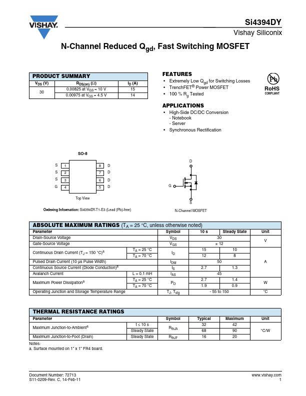
SO-8
D S S S G 1 2 3 4 Top View S Ordering Information: Si4394DY-T1-E3 (Lead (Pb)-free) N-Channel MOSFET 8 7 6 5 D D D D G
ABSOLUTE MAXIMUM RATINGS (TA = 25 °C, unless otherwise noted)
Parameter Drain-Source Voltage Gate-Source Voltage Continuous Drain Current (TJ = 150 °C)a Pulsed Drain Current (10 µs Pulse Width) Continuous Source Current (Diode Conduction)a Avalanch Current Maximum Power Dissipationa Operating Junction and Storage Temperature Range L = 0.1 m H TA = 25 °C TA = 70 °C TA = 25 °C TA = 70 °C Symbol VDS VGS ID IDM IS IAS PD TJ, Tstg 2.7 1.9
- 55 to 150 2.7 45 1.4 0.9 W °C 15 12 50 1.3 10 s 30 ± 12 10 8 A Steady State Unit V
THERMAL RESISTANCE RATINGS
Parameter Maximum Junction-to-Ambient a
Symbol t ≤ 10 s Steady State Steady State Rth JA Rth JF
Typical 32 68 16
Maximum 42 90 20
Unit °C/W
Maximum Junction-to-Foot (Drain) Notes: a. Surface mounted on 1” x 1” FR4 board.
Document Number: 72713 S11-0209-Rev. C, 14-Feb-11
.vishay. 1
Vishay Siliconix
SPECIFICATIONS (TJ = 25 °C, unless otherwise noted)
Parameter Static Gate Threshold Voltage Gate-Body Leakage Zero Gate Voltage Drain Current On-State Drain Currenta Drain-Source On-State Resistancea Forward Transconductancea Diode Forward Voltagea Dynamicb Input Capacitance Output Capacitance Reverse Transfer Capacitance Total Gate Charge Gate-Source Charge Gate-Drain Charge Gate Resistance Turn-On Delay Time Rise Time Turn-Off Delay Time Fall Time Source-Drain Reverse Recovery Time Ciss Coss Crss Qg Qgs Qgd Rg td(on) tr td(off) tf trr IF = 2.9 A, d I/dt = 100 A/µs VDD = 15 V, RL = 15 Ω ID ≅ 1 A, VGEN = 10 V, Rg = 6 Ω f = 1 MHz 0.8 VDS = 15 V, VGS = 4.5 V, ID = 15 A VDS = 15 V, VGS = 0 V, f = 1 MHz 1900 530 120 12.5 3.9 2.1 1.2 13 8 48 13 36 1.8 20 13 75 20 55 ns Ω n C p F VGS(th) IGSS IDSS ID(on)...