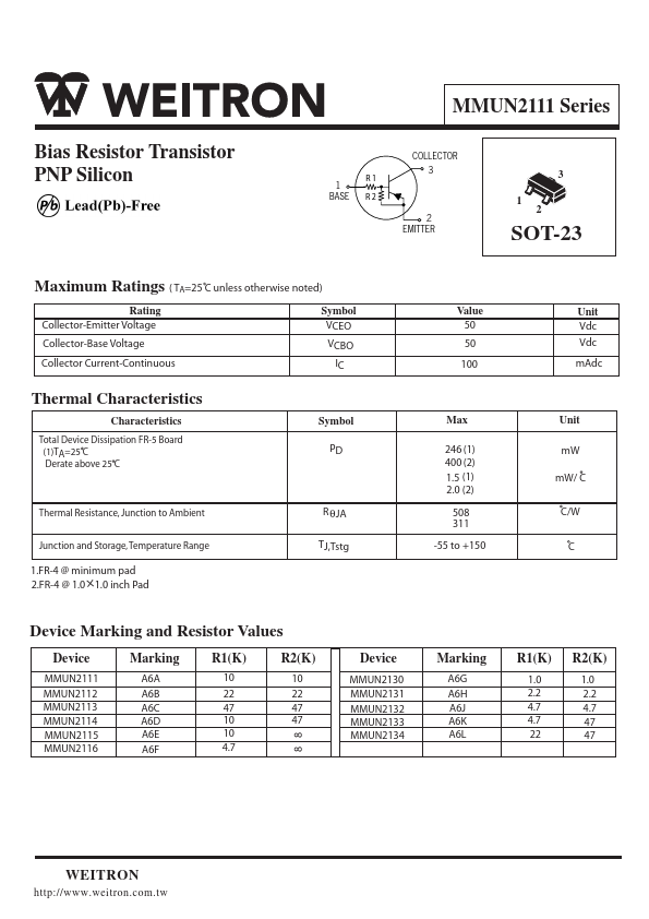
Download the MMUN2112 datasheet PDF.
This datasheet also covers the MMUN2111 variant, as both devices belong to the same bias resistor transistor pnp silicon family and are provided as variant models within a single manufacturer datasheet.
Full PDF Text Transcription for MMUN2112 (Reference)
Note: Below is a high-fidelity text extraction (approx. 800 characters) for
MMUN2112. For precise diagrams, and layout, please refer to the original PDF.
Bias Resistor Transistor PNP Silicon MMUN2111 Series 1 BASE R1 R2 COLLECTOR 3 2 EMITTER 3 1 2 SOT-23 Maximum Ratings ( TA=25 C unless otherwise noted) Rating Collector-Em...
View more extracted text
Maximum Ratings ( TA=25 C unless otherwise noted) Rating Collector-Emitter Voltage Collector-Base Voltage Collector Current-Continuous Symbol VCEO VCBO IC Thermal Characteristics Characteristics Total Device Dissipation FR-5 Board (1)TA=25 C Derate above 25 C Symbol PD Thermal Resistance, Junction to Ambient Junction and Storage, Temperature Range 1.FR-4 @ minimum pad 2.FR-4 @ 1.0 l 1.0 inch Pad R θJA TJ,Tstg Value 50 50 100 Max 246 (1) 400 (2) 1.5 (1) 2.0 (2) 508 311 -55 to +150 Unit Vdc Vdc mAdc Unit mW mW/ C C/W C l 88 Device Marking and Resistor Values Device MMUN2111 MMUN2112 MMUN2113 MMUN2114 MMUN2115 MMUN2116 Marki