Datasheet Summary
Zener Diode Chips for ESD Protection
1. Feature:
1-1 Silicon Zener diode chips for electrostatic discharge (ESD) protection application 1-2 This specification applies to N-Type silicon Zener diode chip Device NO:WT-Z106N-AU4
2. Structure:
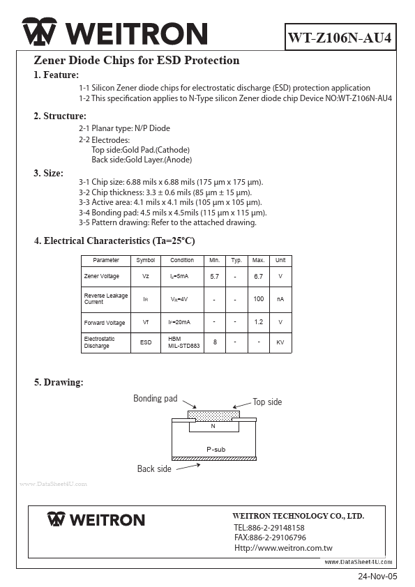
2-1 Planar type: N/P Diode 2-2 Electrodes: Top side:Gold Pad.(Cathode) Back side:Gold Layer.(Anode)
3. Size:
3-1 Chip size: 6.88 mils x 6.88 mils (175 µm x 175 µm). 3-2 Chip thickness: 3.3 ± 0.6 mils (85 µm ± 15 µm). 3-3 Active area: 4.1 mils x 4.1 mils (105 µm x 105 µm). 3-4 Bonding pad: 4.5 mils x 4.5mils (115 µm x 115 µm). 3-5 Pattern drawing: Refer to the attached drawing.
4. Electrical Characteristics (Ta=25ºC)
Parameter Zener Voltage...