Datasheet Summary
Zener Diode Chips for ESD Bidrectional Protection
1. Feature:
1-1 Silicon Zener diode chips for electrostatic discharge(ESD) protection application 1-2 This specification applies to N/P/N-Type silicon Zener diode chip(Vertical) Device NO:WT-Z206V-AU4
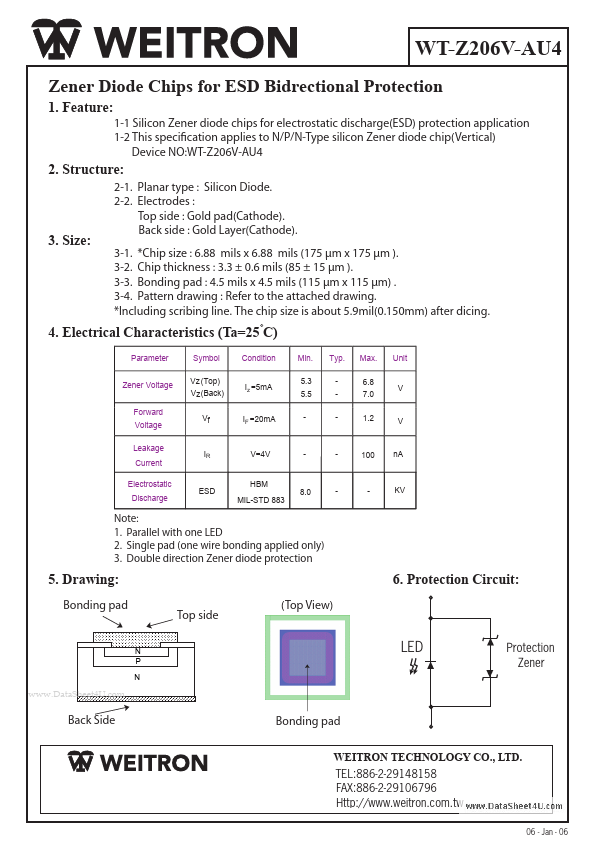
2. Structure:
2-1. Planar type : Silicon Diode. 2-2. Electrodes : Top side : Gold pad(Cathode). Back side : Gold Layer(Cathode). 3-1.
- Chip size : 6.88 mils x 6.88 mils (175 µm x 175 µm ). 3-2. Chip thickness : 3.3 ± 0.6 mils (85 ± 15 µm ). 3-3. Bonding pad : 4.5 mils x 4.5 mils (115 µm x 115 µm) . 3-4. Pattern drawing : Refer to the attached drawing.
- Including scribing line. The chip size is about 5.9mil(0.150mm) after...