Weitron Technology WTL2622
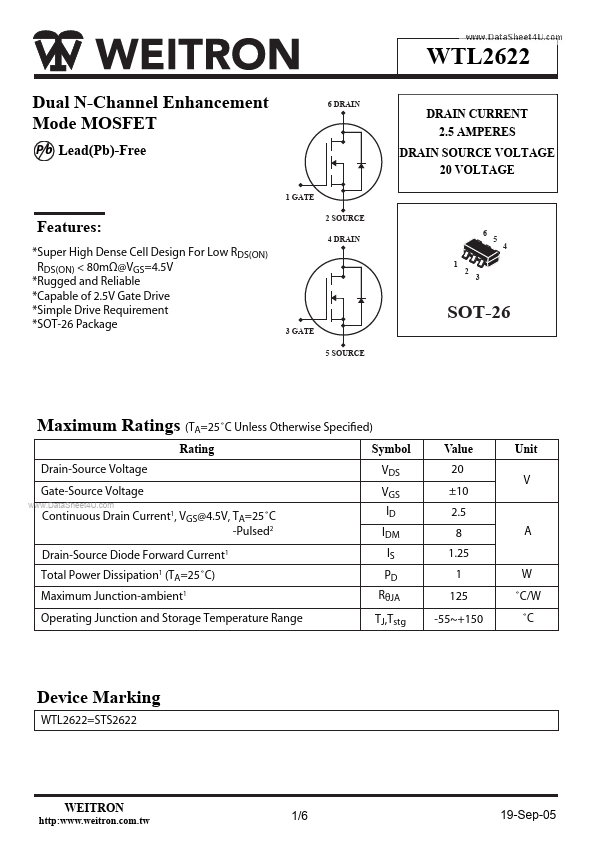
Dual N-Channel Enhancement Mode MOSFET
| Part No. | WTL2622 |
|---|---|
| Datasheet | WTL2622 Download |
| Manufacturer |  Weitron Technology |
| Description | Dual N-Channel Enhancement Mode MOSFET |
| Buy | Stock & Price |
FEATURES
: *Super High Dense Cell Design For Low RDS(ON) RDS(ON) < 80mΩ@VGS=4.5V *Rugged and Reliable *Capable of 2.5V Gate Drive *Simple Drive Requirement *SOT-26 Package 2 SOURCE 4 DRAIN 1 6 5 4 2 3 SOT-26 3 GATE 5 SOURCEMAXIMUM RATINGS
(TA=25˚C Unless Otherwise Specified) Rating Drain-Source Voltage Gate-Source Voltage Symbol VDS VGS ID IDM IS PD RθJA TJ,Tstg Value 20 ±10 2.5 8 1.25 1 125 -55~+150 Unit V Continuous Drain Current1, VGS@4.5V, TA=25˚C -Pulsed2 Drain-Source Diode Forward Current1 A W ˚C/W ˚C Total Power Dissipation1 (TA=25˚C) Maximum Junction-ambient1 Operating Junction and Storage Temperature Range Device Marking WTL2622=STS2622 http: WEITRON 1/6 19-Sep-05 WTL2622ELECTRICAL CHARACTERISTICS
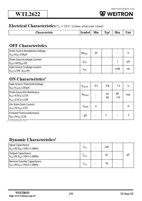
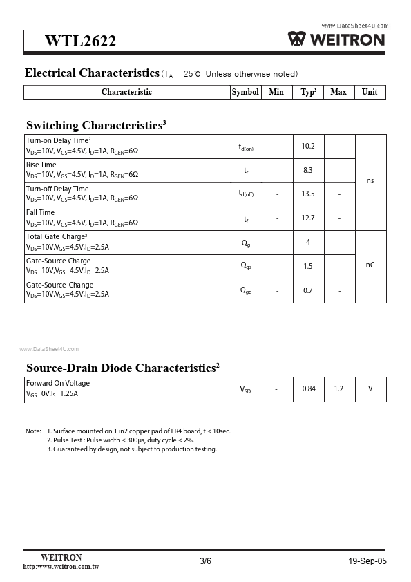
(TA = 25℃ Characteristic Unless otherwise noted) Symbol Min Typ3 Max Unit OFF Characteristics Drain-Source Breakdown Voltage VGS=0,ID=250 μA Drain-SourceLeakage Current VDS=16V,VGS=0V Gate-Source Leakage current VGS=±10V, VDS=0V BVDSS IDSS IGSS 20 1 ±100 V μA nA ON Characteristics2 G...