WD2501
WD2501 is LSI PACKET NETWORK INTERFACE manufactured by Western Digital.
WESTERN DIGITAl.. c o R p o R A TI o N
LSI PACKET NETWORK INTERFACE WD2501/11 SHORT FORM DATA SHEET
Features
- Packet Switching Controller patible with CCITI
Remendation X.2S, Level 2, LAP.
- Programmable Primary Timer (T1) And Retransmission Counter (N2)
- Programmable A-Field Which Provides A Wider Range Of Applications Than Defined By X.25. These Include: DTE-To-DTE Connection, Multipoint, And Loop-Back Testing
- Direct Memory Access (DMA) Transfer: Two Channels; One For Transmit And One For Receive. Send I Receive Data Accessed By Indirect Addressing Method. No External Address Latches Required. Sixteen Output Address Lines.
- Zero Bit Insert And Delete
- Automatic Appending and Testing Of FCS Field
- puter Bus Interface Structure: 8 Bit Bi-
Directional Data Bus. CS, WE, RE-Four Input Address Lines
- DC To
- 1.6M Bitsl SEC Baud Rate if
- TTL patible
- 48 Pin Dual In-Line Packages
- Pin-for-pin patible with WD2511 (LAPB.)
Higher Baud Rates Available By Special Order
APPLICATIONS X.25 PACKET SWITCHING CONTROLLER PART OF DTE OF DCE PRIVATE PACKET NETWORKS oco
'"
:;;
.c a.E.
(/I
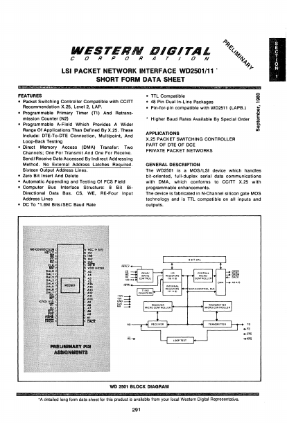
GENERAL DESCRIPTION The WD2501 is a MOS I LSI device which handles bit-oriented, full-duplex serial data munications with DMA, which conforms to CCITT X.25 with programmable enhancements. The device is fabricated in N-Channel silicon gate MOS technology and is TTL patible on all inputs and outputs.
WD 2501 BLOCK DIAGRAM
- %@
- A detailed long form data sheet for this product is available from your local Western Digital Representative.
INTERFACE SIGNAL DESCRIPTION
'PIN...