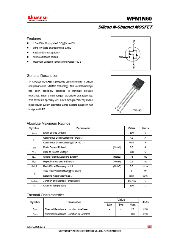
FEATURES
1.3A,600V, RDS(on)(Max8.5Ω)@VGS=10V Ultra-low Gate charge(Typical 9.1nC) Fast Switching Capability 100%Avalanche Tested Maximum Junction Temperature Range(150℃) GENERAL DESCRIPTION
Th is Power MO SFET is produced using Winse mi’s advan ced planar stripe, VDMOS technology. electronic Lamp ballasts based on half bridge and UPS. ABSOLUTE MAXIMUM RATINGS
Symbol VDSS ID IDM VGS EAS EAR dv/dt PD TJ,Tstg TL Drain Source Voltage Continuous Drain Current(@Tc=25℃) Continuous Drain Current(@Tc=100℃) Drain Current Pulsed Gate to Source Voltage Single Pulsed Avalanche Energy Repetitive Avalanche Energy Peak Diode Recovery dv /dt Total Power Dissipation(@Tc=25℃) Derating Factor above 25℃ Junction and Storage Temperature Channel Temperature (Note2) (Note1) (Note3) (Note1) Parameter Value 600 1.3 0.84 5.0 ±30 78 3.9 5.5 5 0.05 -55~150 300 Units V A A A V mJ mJ V/ ns W W/℃ ℃ ℃ Thermal Characteristics Symbol RQJC RQJA Parameter Thermal Resistance , Junction -to -Case Thermal Resistance , Junction-to -Ambient Value Min - Typ - Max 25 120 Units ℃/W ℃/W Rev.A Aug.2011 Copyright@Winsemi Microelectronics Co., Ltd., All right reserved. Winsemi