Description
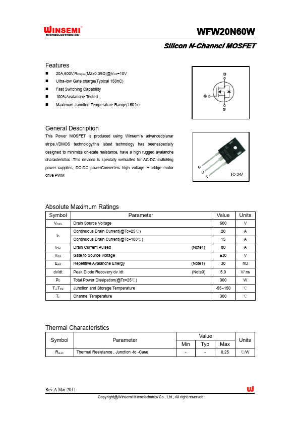
This Power MOSFET is produced using Winsemi's advancedplanar stripe,VDMOS technology.this latest technology has beenespecially designed to minimize on-state resistance, have a high rugged avalanche characteristics .This devices is specially wellsuited for AC-DC switching power supplies, DC-DC powerConverters high voltage H-bridge motor drive PWM Symbol VDSS ID IDM VGS EAR dv/dt PD TJ,Tstg TL Drain Source Voltage Continuous Drain Current(@Tc=25℃) Continuous Drain Current(@Tc=100℃) Drain Current Pulsed Gate to Source Voltage Repetitive Avalanche Energy Peak Diode Recovery dv /dt Total Power Dissipation(@Tc=25℃) Junction and Storage Temperature Channel Temperature (Note1) (Note3) (Note1) Parameter Value 600 20 15 80 ±30 30 5.0 300 -55~150 300 Units V A A A V mJ V/ ns W ℃ ℃ Symbol RQJC Parameter Value Min - Typ - Max 0.25 Units ℃/W Rev.A Mar.2011 Copyright@Winsemi Microelectronics Co., Ltd., All right reserved. Datasheet pdf - http://..net/ .DataSheet.co.kr W20 N60W WF WFW 20N Characteristics Gate leakage current Gate-source breakdown voltage Drain cut -off current Drain -source breakdown voltage Breakdown voltage Temperature coefficient Gate threshold voltage Drain -source ON resistance Forward Transconductance Input capacitance Reverse transfer capacitance Output capacitance Rise time Turn-on time Switching time Fall time Turn-off time Total gate charge(gate-source Qg plus gate-drain) Gate-source charge Gate-drain("miller") Charge Qgs Qgd VGS=10V, nC ID=10A 30 60 40 85 Symbol IGSS V(BR)GSS IDSS V(BR)DSS △BVDSS/ △TJ VGS(th) RDS(ON) gfs Ciss Crss Coss tr ton tf Toff Test Condition VGS=±30V,V DS=0V IG=±10 µA,VDS=0V VDS=600V,V GS=0V VGS=0V,TJ=125℃ ID=250µA,VGS=0V ID=250µA,Referenced to 25℃ VDS=VGS,ID=4mA VGS=10V,ID=10A VDS≥10V,ID=10A VDS=25V, VGS=0V, f=1MHz VGS=10V VDS=300V, ID=10A RG=2.00Ω Min ±30 600 3 11 - Type 0.5 18 4500 140 420 45 20 40 70 Max ±100 200 1000 5 0.39 - Unit nA V µA µA V V/℃ V Ω S pF 60 40 60 90 ns VDS=300V, 150 170 Source-Drain Ratings and Characteristics(Ta=25℃) Characteristics Continuous drain reverse current Forward voltage(diode) Reverse recovery time Reverse recovery charge Symbol IDR VDSF trr Qrr Test Condition IDR=ISA,VGS=0V IDR=10A,VGS=0V, dIDR / dt =100 A / µs Min - Type - Max 20 1.5 250 Unit A V ns µC 1 - Note 1.Pulse Test:Pulse Width≤300us,Duty Cycle≤2% 2.