XM28C020
XM28C020 is 5 Volt/ Byte Alterable E2PROM manufactured by Xicor Inc..
DESCRIPTION
256K x 8 Bit
TYPICAL FEATURES
- -
- -
- -
- -
- -
High Density 2 Megabit (256K x 8) Module Access Time of 150ns at
- 55°C to +125°C Base Memory ponent: Xicor X28C513 Pinout conforms to JEDEC Standard for 2 Megabit E2PROM Fast Write Cycle Times
- 128 Byte Page Write
- Byte or Page Write Cycle: 5ms Typical
- plete Memory Rewrite: 10 Seconds Early End of Write Detection
- DATA Polling
- Toggle Bit Polling Software Data Protection Three Temperature Ranges
- mercial: 0°C to +75°C
- Industrial:
- 40° to +85°C
- Military:
- 55° to +125°C High Rel Module
- 100% MIL-STD-883 pliant ponents Endurance: 100,000 Cycles
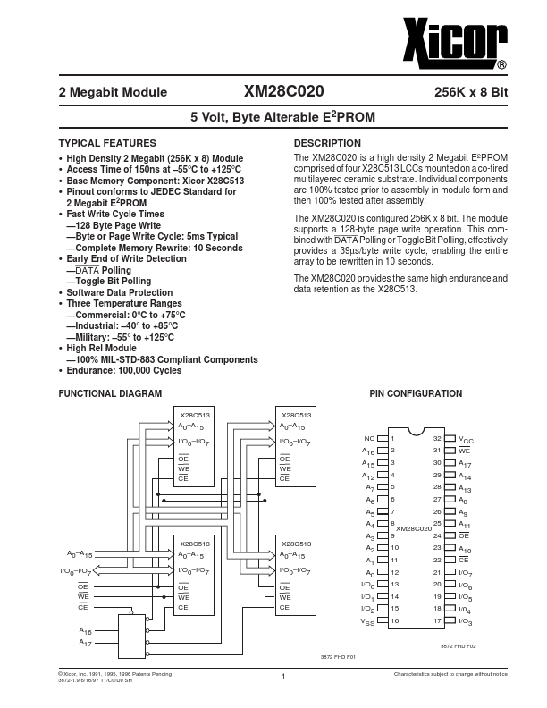
The XM28C020 is a high density 2 Megabit E2PROM prised of four X28C513 LCCs mounted on a co-fired multilayered ceramic substrate. Individual ponents are 100% tested prior to assembly in module form and then 100% tested after assembly. The XM28C020 is configured 256K x 8 bit. The module supports a 128-byte page write operation. This bined with DATA Polling or Toggle Bit Polling, effectively provides a 39µs/byte write cycle, enabling the entire array to be rewritten in 10 seconds. The XM28C020 provides the same high endurance and data retention as the X28C513.
FUNCTIONAL DIAGRAM
X28C513 A0- A15 I/O0- I/O7 OE WE CE X28C513 A0- A15 I/O0- I/O7 OE WE CE
PIN CONFIGURATION
NC A16 A15 A12 A7 A6 A5 A4 A3 A2 A1 A0 I/O0 I/O1 I/O2 VSS
1 2 3 4 5 6 7 8 9 10 11 12 13 14 15 16 XM28C020
32 31 30 29 28 27 26 25 24 23 22 21 20 19 18 17
VCC WE A17 A14 A13 A8 A9 A11 OE A10 CE I/O7 I/O6 I/O5 I/04 I/O3
A0- A15 I/O0- I/O7 OE WE CE A16 A17
X28C513 A0- A15 I/O0- I/O7 OE WE CE
X28C513 A0- A15 I/O0- I/O7 OE WE CE
3872 FHD F02
3872 FHD F01
© Xicor, Inc. 1991, 1995, 1996 Patents Pending 3872-1.9 6/18/97 T1/C0/D0 SH
Characteristics subject to change without notice
PIN DESCRIPTIONS Addresses (A0- A17) The Address inputs select an 8-bit memory location during a read or write operation. Chip Enable (CE) The Chip Enable input must be LOW to enable all read/ write operations....