FEATURES
● In-system programmable 3.3V PROMs for configuration of Xilinx FPGAs - Endurance of 10,000 program/erase cycles - Program/erase over full commercial voltage and temperature range IEEE Std 1149.1 boundary-scan (JTAG) support Simple interface to the FPGA; could be configured to use only one user I/O pin Cascadable for storing longer or multiple bitstreams Dual configuration modes - Serial Slow/Fast configuration (up to 15 mHz). - Parallel Low-power advanced CMOS FLASH process 5 V tolerant I/O pins accept 5 V, 3.3 V and 2.5 V signals. 3.3 V or 2.5 V output capability Available in PC20, SO20, PC44 and VQ44 packages. Design support using the Xilinx Alliance and Foundation series software packages. JTAG command initiation of standard FPGA configuration. DESCRIPTION
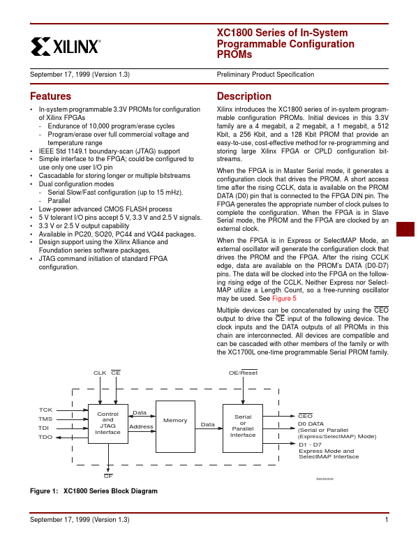
Xilinx introduces the XC1800 series of in-system programmable configuration PROMs. Initial devices in this 3.3V family are a 4 megabit, a 2 megabit, a 1 megabit, a 512 Kbit, a 256 Kbit, and a 128 Kbit PROM that provide an easy-to-use, cost-effective method for re-programming and storing large Xilinx FPGA or CPLD configuration bitstreams. Xilinx Inc