ZVP3310F Overview
Key Specifications
Package: SOT-23-3
Mount Type: Surface Mount
Pins: 3
Height: 1.02 mm
Key Features
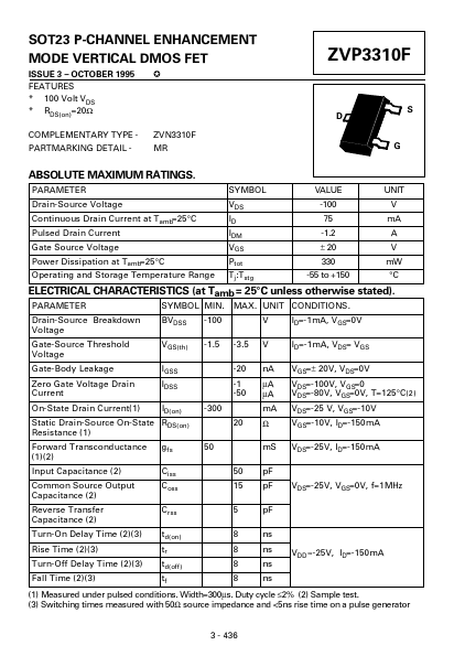
- * 100 Volt VDS * RDS(on)=20Ω COMPLEMENTARY TYPE PARTMARKING DETAIL 7 ZVP3310F D S ZVN3310F MR G
| Part | ZVP3310F |
|---|---|
| Description | P-CHANNEL ENHANCEMENT MODE VERTICAL DMOS FET |
| Manufacturer | Zetex Semiconductors |
| Size | 112.06 KB |
Package: SOT-23-3
Mount Type: Surface Mount
Pins: 3
Height: 1.02 mm
| Seller | Inventory | Price Breaks | Buy |
|---|---|---|---|
| Avnet | 9000 | 3000+ : 0.14758 USD 6000+ : 0.14242 USD 12000+ : 0.14035 USD 24000+ : 0.13829 USD |
View Offer |
| Newark | 3690 | 5+ : 0.978 USD 10+ : 0.64 USD 25+ : 0.574 USD 50+ : 0.508 USD |
View Offer |
| Part Number | Manufacturer | Description |
|---|---|---|
| CBT3253 | Nexperia | Dual 1-of-4 FET multiplexer/demultiplexer |
| TL074C | STMicroelectronics | LOW NOISE J-FET QUAD OPERATIONAL AMPLIFIER |
| CBT3125 | Nexperia | Quadruple FET bus switch |