ZXM63N03X Overview
Key Features
- Low on-resistance
- Fast switching speed
- Low threshold
- Low gate drive
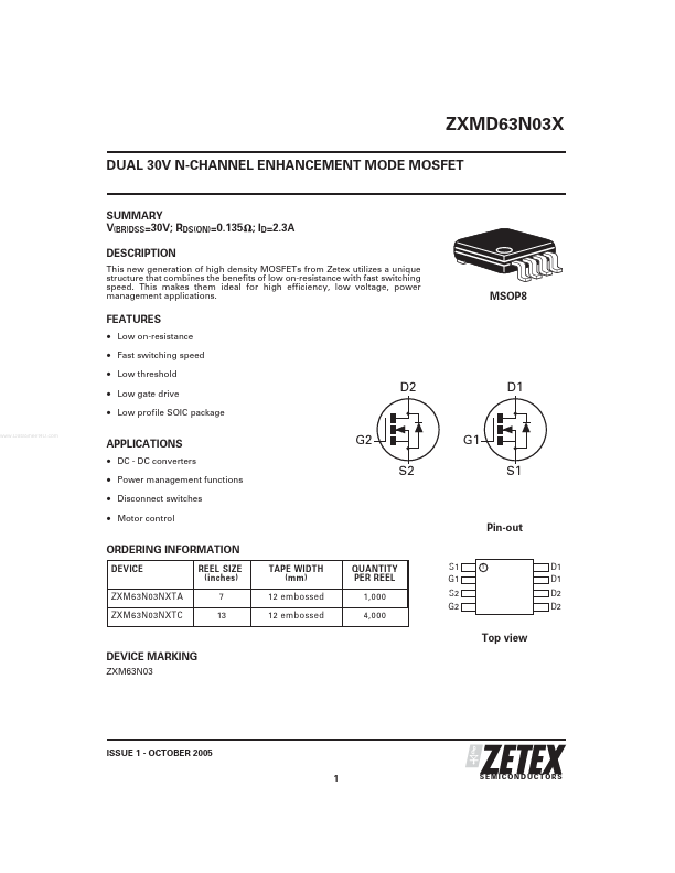
- Low profile SOIC package D2 D1
| Part | ZXM63N03X |
|---|---|
| Description | DUAL 30V N-CHANNEL ENHANCEMENT MODE MOSFET |
| Category | MOSFET |
| Manufacturer | Zetex Semiconductors |
| Size | 355.18 KB |
| Part Number | Manufacturer | Description |
|---|---|---|
| AP9563GH | Advanced Power Electronics Corp | P-CHANNEL ENHANCEMENT MODE POWER MOSFET |
| A2SHB | HAOHAI | N-Channel MOSFET |
| FCPF360N65S3R0L | onsemi | N-Channel MOSFET |