ZXT2M322
ZXT2M322 is MPPS Miniature Package Power Solutions 20V PNP LOW SATURATION SWITCHING TRANSISTOR manufactured by Zetex Semiconductors.
DESCRIPTION
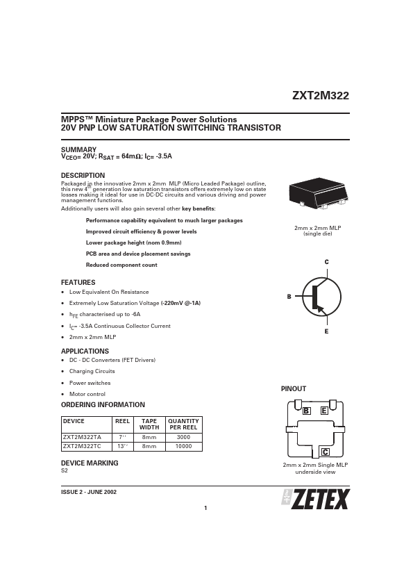
Packaged in the innovative 2mm x 2mm MLP (Micro Leaded Package) outline, this new 4th generation low saturation transistors offers extremely low on state losses making it ideal for use in DC-DC circuits and various driving and power management functions. Additionally users will also gain several other key benefits: Performance capability equivalent to much larger packages Improved circuit efficiency & power levels Lower package height (nom 0.9mm) PCB area and device placement savings Reduced ponent count 2mm x 2mm MLP (single die)
FEATURES
- Low Equivalent On Resistance
- Extremely Low Saturation Voltage (-220m V @-1A)
- h FE characterised up to -6A
- IC= -3.5A Continuous Collector Current
- 2mm x 2mm MLP
APPLICATIONS
- DC
- DC Converters (FET Drivers)
- Charging Circuits
- Power switches
- Motor control
PINOUT
ORDERING INFORMATION
DEVICE ZXT2M322TA ZXT2M322TC REEL 7 13 TAPE WIDTH 8mm 8mm QUANTITY PER REEL 3000 10000 2mm x 2mm Single MLP underside view
DEVICE MARKING
S2
ISSUE 2
- JUNE 2002 1
ABSOLUTE MAXIMUM RATINGS.
PARAMETER Collector-Base Voltage Collector-Emitter Voltage Emitter-Base Voltage Peak Pulse Current (c) Continuous Collector Current (a) Base Current Power Dissipation at TA=25°C (a) Linear Derating Factor Power Dissipation at TA=25°C (b) Linear Derating Factor Power Dissipation at TA=25°C (d) Linear Derating Factor Power Dissipation at TA=25°C (e) Linear Derating Factor Operating and Storage Temperature Range SYMBOL V CBO V CEO V EBO I CM IC IB PD PD PD PD T j :T stg LIMIT -25 -20 -7.5 -6 -3.5 -1000 1.5 12 2.45 19.6 1 8 3 24 -55 to +150 UNIT V V V A A m A W m W/°C W m W/°C W m W/°C W m W/°C °C
THERMAL RESISTANCE
PARAMETER Junction to Ambient (a) Junction to Ambient (b) Junction to Ambient (d) Junction to Ambient (e) SYMBOL R θ JA R θ JA R θ JA R θ JA VALUE 83 51 125 42 UNIT °C/W °C/W °C/W °C/W
NOTES (a) For a single device surface mounted on 10sq cm1oz copper on FR4 PCB in still air conditions with all exposed pads...