Alpha & Omega Semiconductors AOP605L
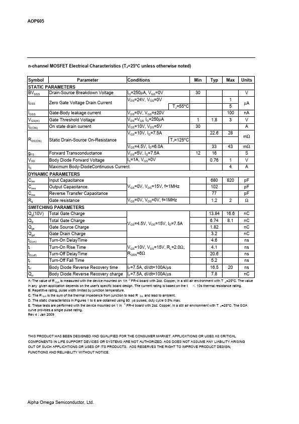
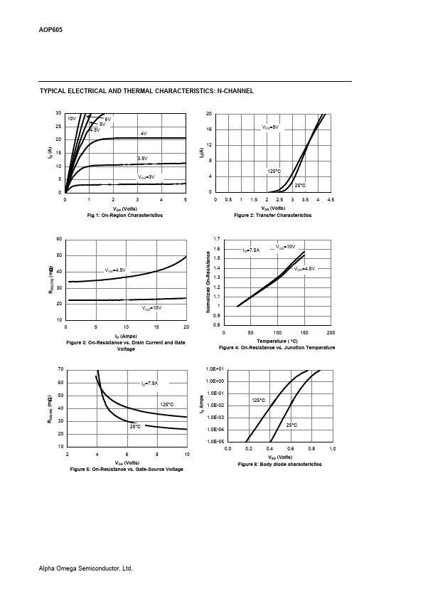
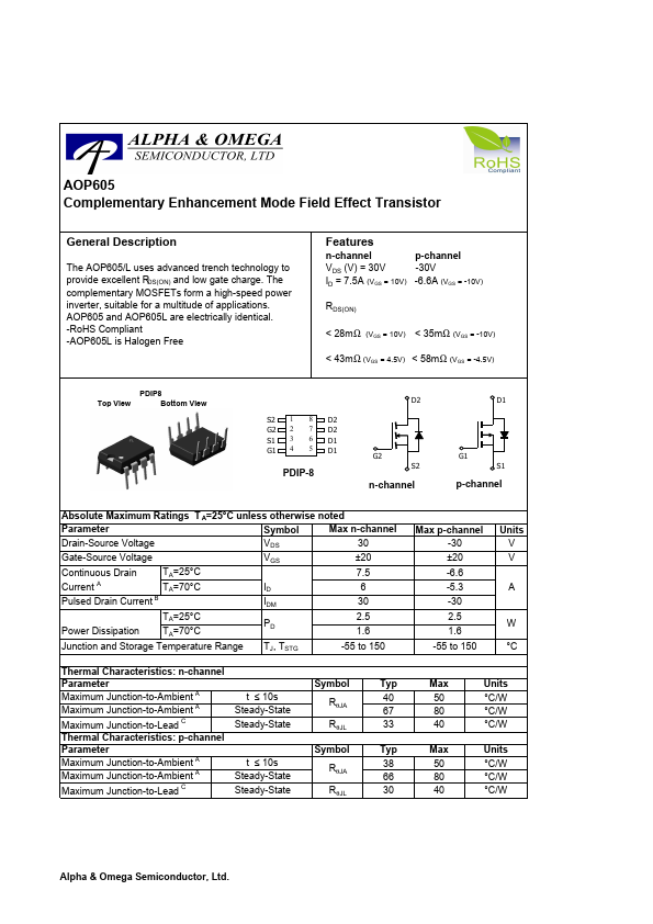
The AOP605/L uses advanced trench technology to provide excellent RDS(ON) and low gate charge. The complementary MOSFETs form a high-speed power inverter, suitable for a multitude of applications. AOP605 and AOP605L are electrically identical.| Part No. | AOP605L |
|---|---|
| Datasheet | AOP605L Download |
| Manufacturer |  Alpha & Omega Semiconductors |
| Description | MOSFET |
| Buy | Stock & Price |
GENERAL DESCRIPTION
AOP605 and AOP605L are electrically identical. -RoHS Compliant -AOP605L is Halogen FreeFEATURES
n-channel VDS (V) = 30V ID = 7.5A (VGS = 10V) p-channel -30V -6.6A (VGS = -10V) RDS(ON) < 28mΩ (VGS = 10V) < 35mΩ (VGS = -10V) < 43mΩ (VGS = 4.5V) < 58mΩ (VGS = -4.5V) PDIP8 Top View Bottom View S2 1 8 D2 G2 2 7 D2 S1 3 6 D1 G1 4 5 D1 PDIP-8 D2 G2 S2 n-channel D1 G1 S1 p-channelABSOLUTE MAXIMUM RATINGS
T A=25°C unless otherwise noted Parameter Symbol Max n-channel Drain-Source Voltage VDS 30 Gate-Source Voltage VGS ±20 Continuous Drain TA=25°C 7.5 Current A TA=70°C ID 6 Pulsed Drain Current B IDM 30 Power Dissipation TA=25°C TA=70°C PD 2.5 1.6 Junction and Storage Temperature Range TJ, TSTG -55 to 150 Thermal Characteristics: n-channel Parameter Maximum Junction-to-Ambient A Maximum Junction-to-Ambient A Symbol Typ t ≤ 10s Steady-State RθJA 40 67 Maximum Junction-to-Lead C Steady-State RθJL 33 Thermal Characteristics: p-channel Parameter Maximum Junction-to-Ambient A Ma...