DTQ1300N03EP
FEATURES
- DT-Trench Power MOSFET
- Fast switching
- Low RDS(ON)
- This is a Pb Free Device
- Ro HS pliant
APPLICATIONS Low Side Load Switch Level Shift Circuits Gate to Source ESD protected, HBM >2KV Portable Applications i.e. DSC, PDA, Cell Phone, etc.
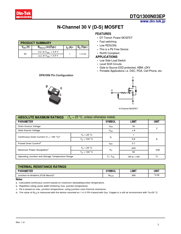
S N-Channel MOSFET
ABSOLUTE MAXIMUM RATINGS (TA = 25 °C, unless otherwise noted)
PARAMETER
SYMBOL
Drain-Source Voltage
Gate-Source Voltage
Continuous Drain Current (TJ = 150 °C)a Pulsed Drain Currentb
TA = 25 °C ID
TA = 100 °C IDM
Maximum Power Dissipationc
TA = 25 °C PD
TA = 100 °C
Operating Junction and Storage Temperature Range
TJ, Tstg
LIMIT 30 ±8 1 0.8 3.7 225 90
-55 to +150
UNIT V
A m W °C
THERMAL RESISTANCE RATINGS
PARAMETER
SYMBOL
LIMIT
UNIT
Junction-to-Ambient (PCB Mount)d
Rth JA
°C/W
Notes a. Calculated continuous current based on maximum allowablejunction temperature. b. Repetitive rating; pulse width limited by max. junction temperature. c. Pd is based on max. junction...