APPLICATIONS
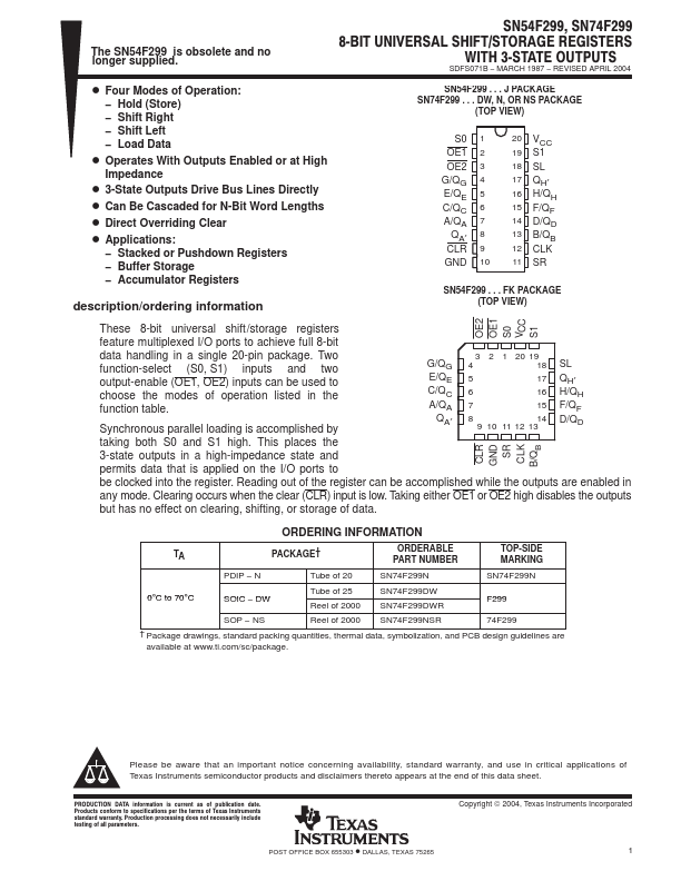
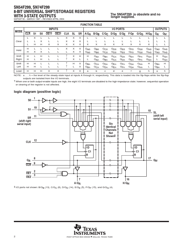
: − Stacked or Pushdown Registers − Buffer Storage − Accumulator Registers description/ordering information SN54F299 . . . J PACKAGE SN74F299 . . . DW, N, OR NS PACKAGE (TOP VIEW) S0 1 OE1 2 OE2 3 G/QG 4 E/QE 5 C/QC 6 A/QA 7 QA′ 8 CLR 9 GND 10 20 VCC 19 S1 18 SL 17 QH′ 16 H/QH 15 F/QF 14 D/QD 13 B/QB 12 CLK 11 SR SN54F299 . . . FK PACKAGE (TOP VIEW) OE2 OE1 S0 VCC S1 These 8-bit universal shift /storage registers feature multiplexed I/O ports to achieve full 8-bit data handling in a single 20-pin package. Two function-select (S0, S1) inputs and two output-enable (OE1, OE2) inputs can be used to choose the modes of operation listed in the function table. Synchronous parallel loading is accomplished by G/QG E/QE C/QC A/QA QA′ 3 2 1 20 19 4 18 5 17 6 16 7 15 8 14 9 10 11 12 13 SL QH′ H/QH F/QF D/QD taking both S0 and S1 high. Reading out of the register can be accomplished while the outputs are enabled in any mode. Clearing occurs when the clear (CLR) input is low. Taking either OE1 or OE2 high disables the outputs but has no effect on clearing, shifting, or storage of data. Texas Instruments