74ACT11646
74ACT11646 is OCTAL BUS TRANSCEIVER/REGISTER manufactured by Texas Instruments.
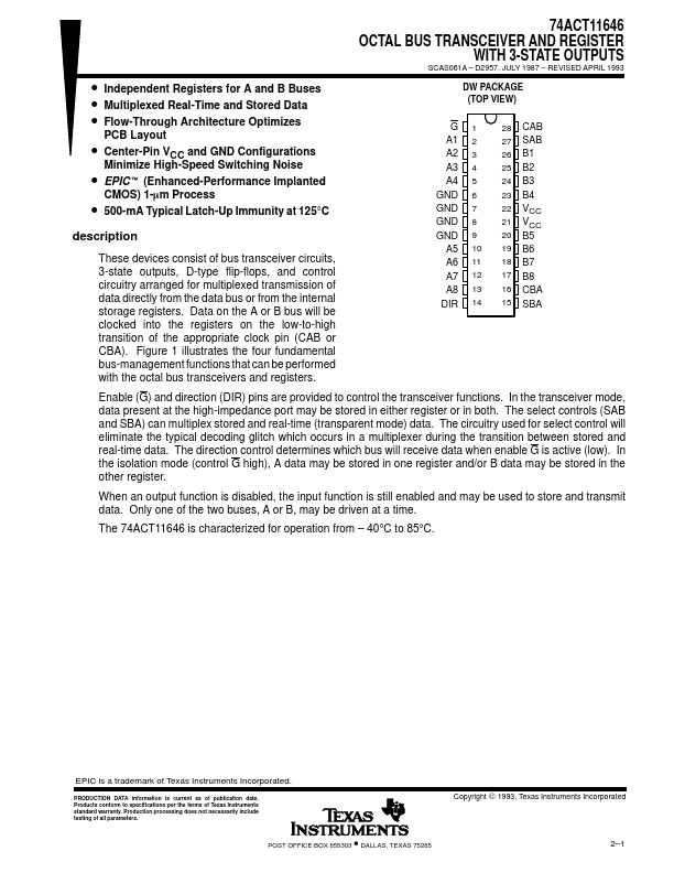
74ACT11646 OCTAL BUS TRANSCEIVER AND REGISTER
WITH 3-STATE OUTPUTS
SCAS061A
- D2957, JULY 1987
- REVISED APRIL 1993
- Independent Registers for A and B Buses
- Multiplexed Real-Time and Stored Data
- Flow-Through Architecture Optimizes
PCB Layout
- Center-Pin VCC and GND Configurations
Minimize High-Speed Switching Noise t- EPIC (Enhanced-Performance Implanted CMOS) 1-mm Process
- 500-mA Typical Latch-Up Immunity at 125°C description
These devices consist of bus transceiver circuits, 3-state outputs, D-type flip-flops, and control circuitry arranged for multiplexed transmission of data directly from the data bus or from the internal storage registers. Data on the A or B bus will be...