Texas Instruments 74HC137
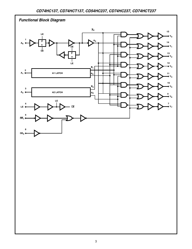
The demultiplexing function is accomplished by using the A0, A1, A2 inputs to select the desired output and using one of the other Output Enable inputs as the data input while holding the other Output Enable input in its active state. Both circuits feature low power consumption usually associated with CMOS circuitry, yet have speeds comparable to low power Schottky TTL logic.| Part No. | 74HC137 |
|---|---|
| Datasheet | 74HC137 Download |
| Manufacturer |  Texas Instruments |
| Description | High-Speed CMOS Logic 3 to 8-Line Decoder/Demultiplexer |
| Buy | Stock & Price |

FEATURES
● Select One of Eight Data Outputs - Active Low for CD74HC137 and CD74HCT137 - Active High for ’HC237 and CD74HCT237● l/O Port or Memory Selector
● Two Enable Inputs to Simplify Cascading
● Typical Propagation Delay of 13ns 15pF, TA = 25oC (CD74HC237) at VCC = 5V,
● Fanout (Over Temperature Range) - Standard Outputs . . . . . . . . . . . . . . . 10 LSTTL Loads - Bus Driver Outputs . . . . . . . . . . . . . 15 LSTTL Loads
● Wide Operating Temperature Range . . . -55oC to 125oC
● Balanced Propagation Delay and Transition Times
● Significant Power Reduction Compared to LSTTL Logic ICs
● HC Types - 2V to 6V Operation - High Noise Immunity: NIL = 30%, NIH = 30%, of VCC at VCC = 5V
● HCT Types - 4.5V to 5.5V Operation - Direct LSTTL Input Logic Compatibility, VIL= 0.8V (Max), VIH = 2V (Min) - CMOS Input Compatibility, Il ≤ 1µA at VOL, VOH
DESCRIPTION
Both circuits have three binary select inputs (A0, A1 and A2) that can be latched by an active High Latch Enable (LE) signal to isolate the outputs from select-input changes.